Page 64 - PEN eBook July 2023
P. 64
Test & Measurement


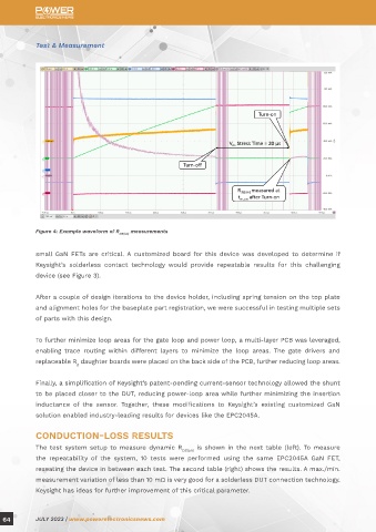
            Figure 4: Example waveform of R DS(on)  measurements


            small GaN FETs are critical. A customized board for this device was developed to determine if
            Keysight’s  solderless  contact  technology  would  provide  repeatable  results  for  this  challenging

            device (see Figure 3).


            After a couple of design iterations to the device holder, including spring tension on the top plate
            and alignment holes for the baseplate part registration, we were successful in testing multiple sets
            of parts with this design.


            To further minimize loop areas for the gate loop and power loop, a multi-layer PCB was leveraged,
            enabling  trace  routing  within  different  layers  to  minimize  the  loop  areas.  The  gate  drivers  and
            replaceable R  daughter boards were placed on the back side of the PCB, further reducing loop areas.
                         g

            Finally, a simplification of Keysight’s patent-pending current-sensor technology allowed the shunt
            to be placed closer to the DUT, reducing power-loop area while further minimizing the insertion
            inductance  of  the  sensor.  Together,  these  modifications  to  Keysight’s  existing  customized  GaN
            solution enabled industry-leading results for devices like the EPC2045A.


            CONDUCTION-LOSS RESULTS

            The test system setup to measure dynamic R         is shown in the next table (left). To measure
                                                           DS(on)
            the  repeatability  of  the  system,  10  tests  were  performed  using  the  same  EPC2045A  GaN  FET,
            reseating the device in between each test. The second table (right) shows the results. A max./min.
            measurement variation of less than 10 mΩ is very good for a solderless DUT connection technology.
            Keysight has ideas for further improvement of this critical parameter.


  64        JULY 2023 | www.powerelectronicsnews.com

