
Page 62 - PEN eBook July 2023
P. 62
Test & Measurement
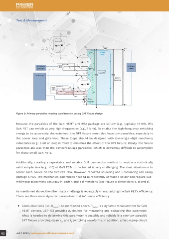
Figure 2: Primary parasitics needing consideration during DPT fixture design
Because the parasitics of the GaN HEMT and BGA package are so low (e.g., typically <1 nH), this
GaN FET can switch at very high frequencies (e.g., 1 MHz). To enable the high-frequency switching
energy to be accurately characterized, the DPT fixture must also have low parasitics, especially in
the power loop and gate loop. These loops should be designed with low-single–digit nanohenry
inductance (e.g., 3 nH or less) in mind to minimize the effect of the DPT fixture. Ideally, the fixture
parasitics are less than the device/package parasitics, which is extremely difficult to accomplish
for these small GaN FETs.
Additionally, creating a repeatable and reliable DUT connection method to enable a statistically
valid sample size (e.g., >10) of GaN FETs to be tested is very challenging. The ideal situation is to
solder each device on the fixture’s PCA. However, repeated soldering and unsoldering can easily
damage a PCA. The mechanical tolerances needed to repeatably contact a solder ball require sub-
millimeter placement accuracy in both X and Y dimensions (see Figure 1: dimensions c, d and e).
As mentioned above, the other major challenge is repeatably characterizing the GaN FET’s efficiency.
There are three main dynamic parameters that influence efficiency:
▶ Conduction loss (i.e., R ): As mentioned above, R is a dynamic measurement for GaN
DS(on) DS(on)
HEMT devices. JEP-173 provides guidelines for measuring and extracting this parameter.
What is needed to determine this parameter repeatably and reliably is a very low parasitic
DPT fixture providing clean V and I switching waveforms. In addition, a fast-clamp circuit
ds d
62 JULY 2023 | www.powerelectronicsnews.com