
Page 61 - PEN eBook July 2023
P. 61
Test & Measurement
efficiency also reduce necessary passive component size (e.g., inductors), further minimizing the
size of the power-converter design. DC/DC converters (12–48 V) made from these GaN FETs enable
the standard 12-V power bus to supply power for these emerging automotive system requirements.
The motor drive (e.g., stepper motors, drones, etc.) is yet another large application for 100-V (and
lower) GaN devices. Low losses often remove the need for heatsinks. GaN enables higher-frequency
PWM signals and significantly reduces switching losses. Higher-frequency switching reduces/
eliminates switch-node oscillations, which often require snubber circuits in Si-based designs.
The are many evolving applications primed to take advantage of GaN’s superior performance
compared with silicon. But the challenges to characterize these devices follow the themes described
above: small size (power density) and higher efficiency.
CHALLENGES CHARACTERIZING LOW-VOLTAGE,
SMALL-FORM–FACTOR GaN POWER DEVICES
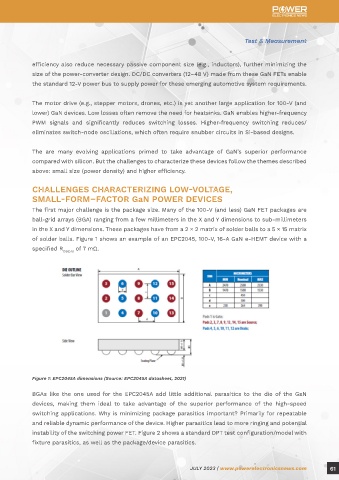
The first major challenge is the package size. Many of the 100-V (and less) GaN FET packages are
ball-grid arrays (BGA) ranging from a few millimeters in the X and Y dimensions to sub-millimeters
in the X and Y dimensions. These packages have from a 2 × 2 matrix of solder balls to a 5 × 15 matrix
of solder balls. Figure 1 shows an example of an EPC2045, 100-V, 16-A GaN e-HEMT device with a
specified R of 7 mΩ.
DS(on)
Figure 1: EPC2045A dimensions (Source: EPC2045A datasheet, 2021)
BGAs like the one used for the EPC2045A add little additional parasitics to the die of the GaN
devices, making them ideal to take advantage of the superior performance of the high-speed
switching applications. Why is minimizing package parasitics important? Primarily for repeatable
and reliable dynamic performance of the device. Higher parasitics lead to more ringing and potential
instability of the switching power FET. Figure 2 shows a standard DPT test configuration/model with
fixture parasitics, as well as the package/device parasitics.
JULY 2023 | www.powerelectronicsnews.com 61