Page 63 - PEN eBook July 2023
P. 63

Test & Measurement


                is needed to settle quickly, enabling a measurement of the clamped V  and I  50 to 500 ns
                                                                                    ds     d
                after the switching event. These techniques will provide the best R     measurement to
                                                                                    DS(on)
                compare against stress voltages and timeframes to characterize the current collapse in

                the GaN FET structure.
             ▶   Switching loss (i.e., t  , t , E  , t  , t , E  ): These parameters are specified in the IEC
                                     d(on)  r  (on)  d(off)  f  (off)
                60747-8  standard  and  are  typically  specified  in  power  FET  datasheets.  The  ability  to
                measure and extract these parameters repeatably and reliably is highly dependent on the
                design of the fixture and the minimization of parasitics. Test conditions typically include
                V , I , V  and sometimes the L    but almost always the gate resistor (R ). R  is one of the
                  ds  d  gs                    load                                    g   g
                main controls of the gate-drive speed and ultimately how hard the device is turned on.
                Most ideally, R  is a small value, allowing for a fast-switching transition. However, if the DPT
                              g
                fixture design is not optimized and has unwanted parasitics, then a larger Rg is needed to

                slow down the switching waveforms to minimize ringing.
             ▶   Drive loss (i.e., Q ): Drive loss is typically the smallest of the losses. Repeatable and reliable
                                g
                measurement  and  calculation  of  gate  charge  (Q )  requires  clean  switching  waveforms,
                                                                 g
                specifically V  and I . Minimal gate-loop parasitics are critical for clean waveforms.
                             gs     g

                                                               REPEATABLE, RELIABLE
                                                               DYNAMIC CHARACTERIZATION
                                                               OF LOW-VOLTAGE GaN FETS

                                                               The  key  to  obtaining  repeatable  and  reliable
                                                               dynamic characterization of small GaN FETs is
                                                               attention to  detail  in the  DPT  fixture  design.
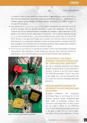
                                                               The EPC2045A described in Figure 1 was used
                                                               as  the  target  DUT.  This  part  exemplifies  the
                                                               100-V GaN FET and the challenges discussed
                                                               previously.


                                                               DESIGN MODIFICATIONS TO
                                                               KEYSIGHT’S CUSTOMIZED GaN
                                                               SOLUTION

                                                               Keysight’s    solderless   DUT     connection
                                                               technology  (Figure  3  and  Figure  9)  for  the
                                                               PD1500A  Dynamic  Power  Analyzer/Double
                                                               Pulse  Tester  is  presented.  However,  this

                                                               connection  technology had not been  tested
                                                               with  as  small  a  device  as  the  EPC2045A
                                                               (1.5 × 2.5 mm), requiring repeatable connections
                                                               to the  gate,  a  single  44.5-µm   round  solder-
                                                                                             2
                                                               ball target. Fixturing and registration of these
            Figure 3: Customized GaN board for EPC2045A


                                                                    JULY 2023 | www.powerelectronicsnews.com         63
   58   59   60   61   62   63   64   65   66   67   68