
Page 20 - EE Times Europe Magazine | April2019
P. 20
20 EE|Times EUROPE
High Power with SiC and GaN
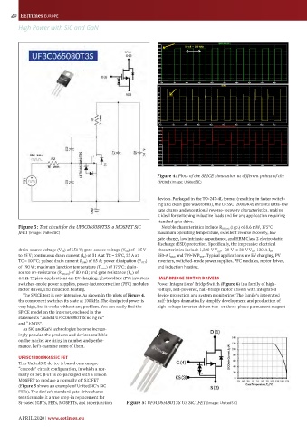
Figure 4: Plots of the SPICE simulation at different points of the
circuit (Image: UnitedSiC)
devices. Packaged in the TO-247-4L format (resulting in faster switch-
ing and clean gate waveforms), the UF3SC120009K4S exhibits ultra-low
gate charge and exceptional reverse-recovery characteristics, making
it ideal for switching inductive loads and for any application requiring
standard gate drive.
Figure 3: Test circuit for the UF3C065080T3S, a MOSFET SiC Notable characteristics include R DS(on) (typ.) of 8.6 mW, 175°C
JFET (Image: UnitedSiC) maximum operating temperature, excellent reverse recovery, low
gate charge, low intrinsic capacitance, and HBM Class 2 electrostatic
discharge (ESD) protection. Specifically, the impressive electrical
drain-source voltage (V DS ) of 650 V; gate-source voltage (V GS ) of –25 V characteristics include 1,200-V V , –20-V to 20-V V GS , 120-A I D ,
DS
to 25 V; continuous drain current (I D ) of 31 A at TC = 25°C, 23 A at 550-A I DM , and 789-W P TOT . Typical applications are EV charging, PV
TC = 100°C; pulsed drain current (I DM ) of 65 A; power dissipation (P TOT ) inverters, switched-mode power supplies, PFC modules, motor drives,
of 190 W; maximum junction temperature (T Jmax ) of 175°C; drain- and induction heating.
source on-resistance (R DS(on) ) of 80 mΩ; and gate resistance (R G ) of
4.5 Ω. Typical applications are EV charging, photovoltaic (PV) inverters, HALF-BRIDGE MOTOR DRIVERS
switched-mode power supplies, power-factor correction (PFC) modules, Power Integrations’ BridgeSwitch (Figure 6) is a family of high-
motor drives, and induction heating. voltage, self-powered, half-bridge motor drivers with integrated
The SPICE test is very intensive. As shown in the plots of Figure 4, device protection and system monitoring. The family’s integrated
the component switches its state at 100 kHz. The dissipated power is half-bridges dramatically simplify development and production of
very high, but it works without any problem. You can easily find the high-voltage inverter-driven two- or three-phase permanent magnet
SPICE model on the internet, enclosed in the
statements “.subckt UF3C065080T3S nd ng ns”
and “.ENDS”.
As SiC and GaN technologies become increas-
ingly popular, the products and devices available
on the market are rising in number and perfor-
mance. Let’s examine some of them.
UF3SC120009K4S SiC FET
This UnitedSiC device is based on a unique
“cascode” circuit configuration, in which a nor-
mally on SiC JFET is co-packaged with a silicon
MOSFET to produce a normally off SiC FET
(Figure 5 shows an example of UnitedSiC’s SiC
FETs). The device’s standard gate-drive charac-
teristics make it a true drop-in replacement for
Si-based IGBTs, FETs, MOSFETs, and superjunction Figure 5: UF3C065080T3S G3 SiC JFET (Image: UnitedSiC)
APRIL 2020 | www.eetimes.eu