
Page 22 - EE Times Europe Magazine | April2019
P. 22
22 EE|Times EUROPE
POWER ELECTRONICS
Wide-Bandgap Application in EV Chargers
By Maurizio Di Paolo Emilio
lectric vehicles (EVs) represent a fundamental factor for the value represents a further advantage for high-voltage circuits because
success of e-mobility, thanks to their reduced environmental it allows both switching and power losses to be reduced, enabling a
impact and lower operating costs compared with traditional particularly compact footprint.
Einternal combustion engine vehicles. While waiting for the EV A further advantage of WBG devices is their ability to generate lower
charging network to reach a capillarity similar to that of common gas temperatures than silicon-based devices operating under the same
stations, electric vehicles must be equipped with on-board charging conditions. In a circuit for high-voltage applications, a SiC component
circuits that ensure high efficiency and long range. can withstand junction temperatures higher than 200°C, compared with
The recharging of electric batteries requires, first of all, a conver- about 150°C for a silicon equivalent. The use of WBG devices in EV char-
sion of the electric power source from alternating current (available gers enables higher switching rates and better energy efficiency, which,
on the electricity distribution network) to direct current. The circuit in turn, translate into more compact modules that are simpler to cool.
topologies used to perform this energy conversion are quite standard, Analog Devices offers a wide selection of small-form-factor isolated
including half-and full-bridge rectifier circuits and the classic “totem gate drivers designed for the higher switching speeds and system size
pole” configuration. constraints required by power switching technologies, such as SiC and
ACHIEVING HIGH EFFICIENCY
A classic EV charger circuit comprises a current rectification stage
followed by a DC/DC converter stage. The rectifier circuit, composed
of diodes with nonlinear characteristics, has a rather low power factor
and a large number of undesired harmonic components. A high level
of efficiency can be achieved only through careful design of the power
factor correction (PFC) circuit.
To improve the power factor and reduce harmonic distortion, a
solution based on active power factor correction (APFC) is commonly
adopted. APFC is essential for an active switching circuit that receives
a rectified voltage at its input and boosts that value until it reaches a
DC set value, checking that the line current maintains the desired sinu-
soidal waveform. In principle, in an ideal PFC circuit, the input current
“follows” the input voltage, behaving like a pure resistor and without
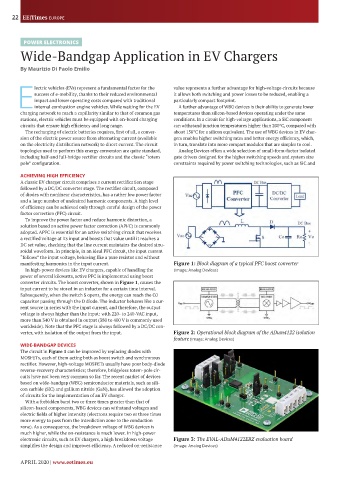
manifesting harmonics in the input current. Figure 1: Block diagram of a typical PFC boost converter
In high-power devices like EV chargers, capable of handling the (Image: Analog Devices)
power of several kilowatts, active PFC is implemented using boost
converter circuits. The boost converter, shown in Figure 1, causes the
input current to be stored in an inductor for a certain time interval.
Subsequently, when the switch S opens, the energy can reach the C0
capacitor passing through the D diode. The inductor behaves like a cur-
rent source in series with the input current, and therefore, the output
voltage is always higher than the input: with 220- to 240-VAC input,
more than 340 V is obtained in output (380 to 400 V is commonly used
worldwide). Note that the PFC stage is always followed by a DC/DC con-
verter, with isolation of the output from the input. Figure 2: Operational block diagram of the ADum4122 isolation
feature (Image: Analog Devices)
WIDE-BANDGAP DEVICES
The circuit in Figure 1 can be improved by replacing diodes with
MOSFETs, each of them acting both as boost switch and synchronous
rectifier. However, high-voltage MOSFETs usually have poor body-diode
reverse-recovery characteristics; therefore, bridgeless totem-pole cir-
cuits have not been very common so far. The recent market of devices
based on wide-bandgap (WBG) semiconductor materials, such as sili-
con carbide (SiC) and gallium nitride (GaN), has allowed the adoption
of circuits for the implementation of an EV charger.
With a forbidden band two or three times greater than that of
silicon-based components, WBG devices can withstand voltages and
electric fields of higher intensity (electrons require two or three times
more energy to pass from the interdiction zone to the conduction
zone). As a consequence, the breakdown voltage of WBG devices is
much higher, while the on-resistance is much lower. In high-power
electronic circuits, such as EV chargers, a high breakdown voltage Figure 3: The EVAL-ADuM4122EBZ evaluation board
simplifies the design and improves efficiency. A reduced on-resistance (Image: Analog Devices)
APRIL 2020 | www.eetimes.eu