
Page 19 - EE Times Europe Magazine | April2019
P. 19
EE|Times EUROPE 19
POWER ELECTRONICS
High Power with SiC and GaN
By Giovanni Di Maria
he wide-bandgap (WBG) semiconductor materials silicon
carbide (SiC) and gallium nitride (GaN) offer better thermal
conductivity, higher switching speeds, and physically smaller
T devices than traditional silicon. The poor parasitic-diode
characteristics of silicon MOSFETs produce high current peaks
and high electromagnetic interference (EMI). The WBG materials
have about 10× better conduction and switching properties than Si.
Consequently, WBG technology is a natural fit for power electronics,
particularly for electric cars, because the SiC and GaN components
are smaller, faster, and more efficient than their silicon counterparts.
INCREASINGLY POWERFUL COMPONENTS
Among the positive aspects and improvements of SiC and GaN semi-
conductors over Si-based MOSFETs and IGBTs, the materials ensure
lower losses, work with higher switching frequencies, endure much
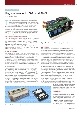
higher operating temperatures, are more robust in difficult environ- Figure 2: A silicon carbide inverter (Image: PED-Board)
ments, and offer higher breakdown voltages.
The electronics sector is moving toward larger high-voltage
batteries with shorter charging times and reduced losses. The new APPLICATIONS
materials are therefore very useful. Wide-bandgap devices work smoothly at high temperatures, high
switching speeds, and low losses. For this reason, they are ideal for
SiC, GaN, OR SILICON? military and industrial applications. Their main use is with bridge
Wide-bandgap power devices (Figure 1) are expensive, and in some circuits for high power, used in inverters (Figure 2), Class D audio
designs, the cost/performance considerations will not work in WBG’s amplifiers, and more. For high-power applications, robustness against
favor. Designers must weigh cost and performance compromises short-circuit transients and surges is a critical consideration.
and, in some cases, evaluate substrates against each other. The inverter that controls the motor in an electric vehicle (EV) is
The first SiC devices to be made available were simple diodes, but an example of a system that can take advantage of WBG devices. The
the material technology has since improved to allow the production main function of the inverter is to convert a DC voltage to a three-
of JFETs, MOSFETs, and bipolar transistors. GaN came after SiC and, phase AC waveform in order to operate the car engine. Because the
in theory, is faster than SiC and allows higher switching speeds. But inverter converts battery energy into alternating current, the lower
GaN adoption has been slow because of the material’s high cost and the losses during this conversion, the more efficient the system will
reliability problems. be. The higher conductivity and higher switching frequency of SiC
GaN voltages are currently limited to about 650 V. SiC voltages devices compared with silicon reduce power loss because less energy
are commonly from about 650 V to 1,200 V but can range higher. is dissipated as heat. Ultimately, the increased efficiency of SiC-based
SiC is widely used in the production of components and is cheaper, inverters will result in greater EV autonomy.
stronger, and more reliable than GaN. From a packaging point of A key element that acts as an interface between the controller and
view, SiC devices are available in TO-247 and TO-220 formats. This the power device is the gate driver. Gate driver design is always prob-
allows a quick and simple replacement of components, even in lematic for electronics designers who adopt new devices, and it
existing projects, with many immediate advantages. GaN devices is important to understand how to drive SiC and GaN power devices.
use surface-mount packages, with consequential limits of use. One The SiC MOSFET transistor must be operated with a higher gate
factor that gives SiC an advantage in industrial systems is its high voltage and must exhibit efficient voltage derivation over time
reliability in overvoltage conditions. Conversely, the maximum volt- (dV/dt) to achieve fast switching times. DC/DC converters also need
age should not be exceeded for GaN devices. to be designed to accommodate new components, such as SiC
MOSFETs. They must have asymmetrical out-
puts for controlling SiC drivers. Insulation
and parasitic capacitance are also important
factors to consider in the design.
SPICE MODELS
Electronic components with SiC and GaN
technology are increasingly popular, on both
an industrial and a commercial level. For this
reason, SPICE models for electronic simula-
tions are proliferating on the internet.
Figure 3 presents a schematic of a test
circuit for the UF3C065080T3S SiC FET,
produced by UnitedSiC. The electrical charac-
Figure 1: Half-bridge SiC (left) and GaN devices (Image: Wolfspeed) teristics of this component are truly stunning:
www.eetimes.eu | APRIL 2020