
Page 24 - EE Times Europe Magazine | April2019
P. 24
24 EE|Times EUROPE
Wide-Bandgap Application in EV Chargers
GaN. These isolated gate drivers are based on ADI’s proven iCoupler combine the outputs from the V OUT and V OUT_SRC pins, one isolated gate
isolation technology, combined with high-speed CMOS and monolithic driver is able to have two easily selectable slew rates.
transformer technology. The ADuM4122 device, an isolated dual-out- The EVAL-ADuM4122EBZ board tests the propagation delay, drive
put driver, provides 5-kV RMS true galvanic isolation between the input strength, slew rate selection, and input logic of the device.
and output regions.
Gate drivers are required for achieving fast rise times for switching WIRELESS CHARGING
device gates. As shown in Figure 2, ADuM4122 achieves isolation Wireless EV charging uses an inductor, usually placed under the
between the control side and the output side of the gate driver by asphalt, and a receiver onboard the vehicle. Charging occurs automati-
using a high-frequency carrier that transmits data across the isolation cally through magnetic plates that continuously recharge the batteries,
barrier with iCoupler chip-scale transformer coils separated by layers of whether the vehicle is standing still or in motion.
polyimide isolation. In the area of wireless power transfer, engineers need solutions with
The EVAL-ADuM4122EBZ evaluation board (Figure 3) supports the high-power and high-efficiency GaN-based approaches. GaN Systems’
ADuM4122 isolated gate driver with slew rate control. The evaluation broad portfolio of transistors provides high-power wireless charging
board supplies jumpers and screw terminals to configure different drive solutions to design smaller, cheaper, and more efficient power systems
conditions, accepting both square waves and DC values on the V and for demanding applications. ■
IN+
SRC pins. The SRC pin controls whether the V OUT_SRC pin is either set to
high-Z or follows the logic of the user-supplied pulse-width modu- Maurizio Di Paolo Emilio is a staff correspondent at AspenCore,
lation (PWM) input at V . When the external series gate resistors editor of Power Electronics News, and editor-in-chief of EEWeb.
IN+
POWER ELECTRONICS
Wide-Bandgap Semiconductors
Find Homes in Space
By Maurizio Di Paolo Emilio
ide-bandgap (WBG) semiconductors, such as gallium
nitride (GaN) and silicon carbide (SiC), are proving to
be the most promising materials in the field of power
Welectronics since silicon was introduced. These materials
have several advantages over traditional silicon-based technology, such
as the ability to manage high power levels, insensitivity to radiation,
high-temperature operation, high switching frequencies, low noise, low
power losses, and high efficiency.
WBG semiconductors are of strategic importance to the develop-
ment of next-generation space-borne systems. Gallium nitride, in its
enhanced-mode version (eGaN), is widely used in the development of
FETs and HEMTs for space applications.
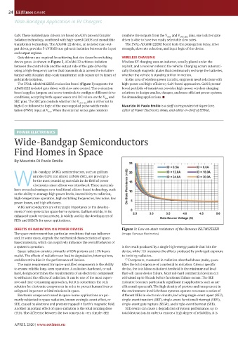
EFFECTS OF RADIATION ON POWER DEVICES Figure 1: Low on-state resistance of the Renesas ISL70023SEH
The space environment has particular conditions that can influence (Image: Renesas Electronics)
and, in some cases, degrade the mechanical characteristics of space-
based materials, which can negatively influence the overall behavior of
a system’s operation. is the result produced by a single high-energy particle that hits the
Space radiation consists primarily of 85% protons and 15% heavy device, while TID measures the effects produced by prolonged exposure
nuclei. The effects of radiation can lead to degradation, interruptions, to ionizing radiation.
and discontinuities in the performance of devices. TID exposure, measured in radiation-absorbed doses (rads), quan-
The main requirement for space-qualified components is the ability tifies the total exposure of a material to radiation. Given a specific
to ensure reliable long-term operation. A radiation-hardened, or rad- device, the total dose radiation threshold is the minimum rad level
hard, design determines the requirements of an electronic component that will cause device failure. Most rad-hard commercial devices can
to withstand the effects of radiation. It can be one of the most expen- withstand up to 5 krads before functional failure occurs. The SEE
sive and time-consuming approaches, but it is sometimes the only indicator becomes particularly significant in applications such as sat-
solution for electronic components in order to protect human lives or ellites and spacecraft. The high density of protons and ions present in
safeguard important orbital missions in space. the environment in which these systems operate can cause a series of
Electronic components used in space-borne applications are pri- different SEEs in electronic circuits, including single-event upset (SEU),
marily subjected to space radiation, known as single-event effect, or single-event transient (SET), single-event functional interrupt (SEFI),
SEE, caused by electrons and protons trapped in Earth’s magnetic field. single-event gate rupture (SEGR), and single-event burnout (SEB).
Another important effect of space radiation is the total ionizing dose SEE events can cause a degradation of system performance, up to
(TID). The difference between the two concepts is very simple: SEE total destruction. In order to ensure a high degree of reliability, it is
APRIL 2020 | www.eetimes.eu