
Page 55 - EETEurope FlipBook February
P. 55
EE|Times EUROPE 55
Will Fan-Out Wafer-Level Packaging Keep Moore’s Law Valid?
as the back of the chip is fully exposed, facil- as logic speeds rise and can dramatically assembly and test outfits to verify the full
itating heat removal. The RDL-first approach alter signal timing and characteristics. Thus, packaged chip design. The EDA companies
allows the use of known-good die in its fabri- developers seeking to use advanced packag- are also stepping up to develop design and
cation, increasing yield. ing techniques will need to ensure that their verification tools that can support these
In performance, the face-down approach has simulations and design verification efforts advanced packaging requirements.
a shorter connection path than the face-up and include the package as well as the chip design Either way, the role of advanced packaging
RDL-first approaches (Figure 2). The two latter to ensure success. will continue to grow as the industry keeps
approaches have copper pillars, which extend Chip vendors are starting to develop pushing to keep Moore’s Law valid as long as
the connection to the RDL, as well as a layer their own in-house tools that integrate possible. The demand for smaller, faster, more
of material under the chip that adds parasitic the package and chip design into a single capable chips and systems will continue, and
capacitance between the connections, affecting process flow for their customers. However, packaging now looks to be the new frontier
their high-frequency performance. in-house tools may limit designer choices that developers will need to explore. ■
for the chips made with vendor processes.
NEW TOOLS FOR ADVANCED PACKAGING Those who want to mix chips from different Richard Quinnell is a retired engineer and
Such subtle parasitic effects due to the pack- processes may need to depend instead on writer and the former editor-in-chief of EDN.
age’s fabrication are increasingly important tools that are available through outsourced This article was originally published on EDN.
SPECIAL REPORT: ADVANCED IC PACKAGING
Five Keys to Next-Generation
IC Packaging Design
By Keith Felton
or many applications, next-generation IC packaging is the best
path to achieve silicon scaling, functional density, and hetero-
geneous integration while reducing the overall package size.
F Heterogeneous and homogeneous integration technologies offer
a path to enhanced device functionality, faster time to market, and
silicon yield resiliency.
Multiple integration technology platforms have emerged that allow
for cost, size, performance, and power optimizations to satisfy the
needs of multiple markets, such as mobile computing, automotive, 5G,
artificial intelligence, augmented reality and virtual reality, high-
performance computing, IoT, medical, and aerospace. However, these
packages present unique challenges for traditional package design
tools and methodologies. Design teams must work together to verify
and optimize the entire system, not just the individual elements.
Traditional IC packaging substrate design is typically very simi-
lar to a small-scale laminate and/or buildup-based PCB. It is often
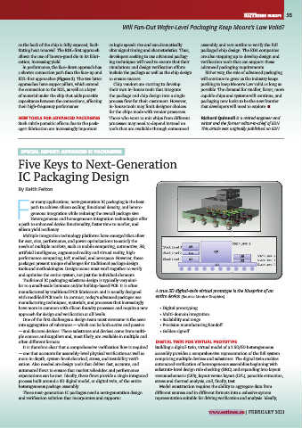
manufactured by traditional PCB fabricators and is usually designed A true 3D digital-twin virtual prototype is the blueprint of an
with modified PCB tools. In contrast, today’s advanced packages use entire device. (Source: Mentor Graphics)
manufacturing techniques, materials, and processes that increasingly
have more in common with silicon foundry processes and require a new • Digital prototyping
approach for design and verification at all levels. • Multi-domain integration
One of the first challenges a design team must overcome is the accu- • Scalability and range
rate aggregation of substrates — which can be both active and passive • Precision manufacturing handoff
— and discrete devices. These substrates and devices come from multi- • Golden signoff
ple sources and suppliers and, most likely, are available in multiple and
often different formats. DIGITAL TWIN FOR VIRTUAL PROTOTYPE
It is therefore clear that a comprehensive verification flow is required Building a digital-twin, virtual model of a 2.5D/3D heterogeneous
— one that accounts for assembly-level physical verification as well as assembly provides a comprehensive representation of the full system
more in-depth, system-level electrical, stress, and testability verifi- comprising multiple devices and substrates. The digital twin enables
cation. Also needed are design tools that deliver fast, accurate, and automated verification of heterogeneous assemblies beginning with
automated flows to ensure that market schedules and performance substrate-level design rule checking (DRC) and expanding into layout
expectations can be met. Ideally, these flows provide a single integrated versus schematic (LVS), layout versus layout (LVL), parasitic extraction,
process built around a 3D digital model, or digital twin, of the entire stress and thermal analysis, and, finally, test.
heterogeneous package assembly. Model construction requires the ability to aggregate data from
These next-generation IC packages need a next-generation design different sources and in different formats into a cohesive system
and verification solution that incorporates and supports: representation suitable for driving verification and analysis. Ideally,
www.eetimes.eu | FEBRUARY 2021