
Page 54 - EETEurope FlipBook February
P. 54
54 EE|Times EUROPE
SPECIAL REPORT: ADVANCED IC PACKAGING
Will Fan-Out Wafer-Level Packaging Keep
Moore’s Law Valid?
By Richard Quinnell
oore’s Law in process technology
is on its last legs, so advanced
packaging is taking up the baton.
MAdvanced techniques such as
fan-out wafer-level packaging (FOWLP) allow
increased component density, boost perfor-
mance, and help solve chip I/O limitations.
The key to using such techniques successfully,
however, is to include the package in the chip
design from the start.
For decades, semiconductor processing
technology has steadily pushed feature sizes
down from tens of microns to single-digit
nanometers, effectively doubling component
density every 18 months. At the same time,
however, design and fabrication costs have
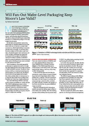
risen, threshold margins have narrowed, and Figure 1: Variations in FOWLP technology include mold-first and RDL-first assembly
a host of other challenges have appeared options. (Source: Micromachines)
to impede further progress. Furthermore,
increased transistor density in individual
chips has created problems in interconnecting FACE-UP AND FACE-DOWN APPROACHES to expose the pillars before attaching the RDL
them, such as limiting I/O pin count and chip- There are several variations of FOWLP, each and forming the solder balls.
to-chip interconnect speed. one using slightly different fabrication In the RDL-first approach, the RDL attaches
These limitations are proving especially steps available from a variety of vendors to the carrier using a temporary release layer,
problematic in applications such as AI edge (Figure 1). The FOWLP assembly can be and the die attaches to the RDL. The assem-
and cloud systems that need massive amounts created using a mold-first process, with chips bly then gets over-molded, the carrier gets
of high-bandwidth memory. To address these mounted face-down or face-up, or by using released, and the solder balls get formed. The
issues as well as to continue improving com- an RDL-first assembly. final step for either approach is to separate
ponent density, the industry has developed In the mold-first approach, the chip die the assemblies, which were formed en masse
several advanced packaging technologies attaches to a carrier using a temporary bond- into individual devices.
that allow multiple chips to interconnect in ing or thermal release layer, which is then The different approaches provide different
a compact, high-performance package that molded into a package. If the die is attached cost/performance tradeoffs. The mold-first,
functions on a board as a single component. face-down, the next steps are to release the face-down approach avoids the need for
One such technology, FOWLP, is already temporary layer, attach the RDL, and form fabricating the copper pillars and for the back
used in volume production for mobile devices. the solder balls that complete the package. If grinding, so it has a lower fabrication cost. It
The FOWLP packaging process involves the die is attached face-up, some additional is best suited for low-I/O–count applications;
mounting individual chips on an interposer steps are needed. however, there are issues with die shift, wafer
substrate called the redistribution layer First, the individual die I/O connections warpage, and the like that limit its usage for
(RDL), which provides the interconnections must be extended by adding copper pillars to complex multi-chip packaging.
between chips and with the I/O pads, all pack- them before over-molding. After the molding, The face-up approach reduces those issues
aged in a single over-molding. the back of the molding must be ground away and has an advantage in thermal management,
Figure 2: The choice of FOWLP approach can affect trace length and create parasitic effects that must be accounted for in the chip’s
design. (Source: Micromachines)
FEBRUARY 2021 | www.eetimes.eu