
Page 50 - EETEurope FlipBook February
P. 50
50 EE|Times EUROPE
SPECIAL REPORT: ADVANCED IC PACKAGING
Heterogeneous Integration and the Evolution
of IC Packaging
By Gareth Kenyon
eterogeneous integration tech-
nology refers to the integration of
separately manufactured compo-
Hnents into a higher-level assembly,
or system-in-package, that in the aggre-
gate provides enhanced functionality and
improved operating characteristics. In this
context, a component can be taken to mean
any unit, such as a microelectromechanical
system, assembled package for high-
bandwidth memory — such as passive compo-
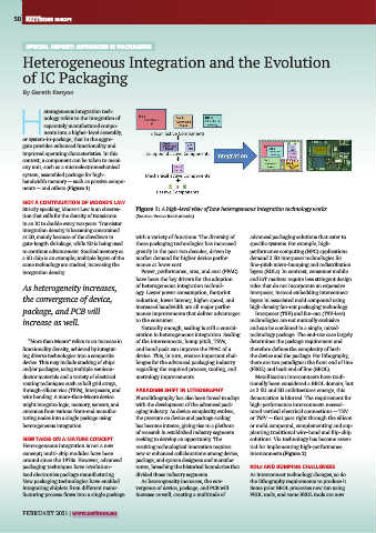
nents — and others (Figure 1).
NOT A CONTINUATION OF MOORE’S LAW
Strictly speaking, Moore’s Law is an observa- Figure 1: A high-level view of how heterogeneous integration technology works
tion that calls for the density of transistors (Source: Veeco Instruments)
in an IC to double every two years. Transistor
integration density is becoming constrained
at 2D, mainly because of the slowdown in with a variety of functions. The diversity of advanced packaging solutions that cater to
gate-length shrinkage, while 3D is being used these packaging technologies has increased specific systems. For example, high-
to continue advancement. Stacked memory as greatly in the past two decades, driven by performance computing (HPC) applications
a 3D chip is an example; multiple layers of the market demand for higher device perfor- demand 2.5D interposer technologies for
same technology are stacked, increasing the mance at lower cost. fine-pitch micro-bumping and redistribution
integration density. Power, performance, area, and cost (PPAC) layers (RDLs). In contrast, consumer mobile
have been the key drivers for the adoption and IoT markets require less stringent design
As heterogeneity increases, of heterogeneous integration technol- rules that do not incorporate an expensive
interposer, instead embedding interconnect
ogy. Lower power consumption, footprint
the convergence of device, reduction, lower latency, higher speed, and layers in associated mold compound using
package, and PCB will increased bandwidth are all major perfor- high-density fan-out packaging technology.
mance improvements that deliver advantages
Interposer (TSV) and fan-out (TSV-less)
increase as well. to the consumer. technologies are not mutually exclusive
Naturally enough, scaling is still a consid- and can be combined in a single, mixed-
eration in heterogeneous integration. Scaling technology package. The end-use case largely
“More than Moore” refers to an increase in of the interconnects, bump pitch, TSVs, determines the package requirement and
functionality density, achieved by integrat- and bond pads can improve the PPAC of a therefore defines the complexity of both
ing diverse technologies into a composite device. This, in turn, creates important chal- the device and the package. For lithography,
device. This may include stacking of chips lenges for the advanced packaging industry there are two paradigms: the front end of line
and/or packages, using multiple semicon- regarding the required process, tooling, and (FEOL) and back end of line (BEOL).
ductor materials and a variety of electrical metrology improvements. Metallization interconnects have tradi-
routing techniques such as ball grid arrays, tionally been considered a BEOL domain, but
through-silicon vias (TSVs), interposers, and PARADIGM SHIFT IN LITHOGRAPHY as 2.5D and 3D architectures emerge, this
wire bonding. A more-than-Moore device Photolithography has also been forced to adapt demarcation is blurred. The requirement for
might integrate logic, memory, sensors, and with the development of the advanced pack- high-performance interconnects necessi-
antennas from various front-end manufac- aging industry. As device complexity evolves, tated vertical electrical connections — TSV
turing nodes into a single package using the pressure on device and package scaling or TMV — that pass right through the silicon
heterogeneous integration. has become intense, giving rise to a plethora or mold compound, complementing and sup-
of research in established industry segments planting traditional wire-bond and flip-chip
NEW TAKES ON A MATURE CONCEPT seeking to develop an opportunity. The solutions. Via technology has become essen-
Heterogeneous integration is not a new resulting technological innovation requires tial for implementing high-performance
concept; multi-chip modules have been new or enhanced collaborations among device, interconnects (Figure 2).
around since the 1970s. However, advanced package, and system designers and manufac-
packaging techniques have revolution- turers, breaching the historical boundaries that RDLs AND BUMPING CHALLENGES
ized electronics package manufacturing. divided those industry segments. As interconnect technology changes, so do
New packaging technologies have enabled As heterogeneity increases, the con- the lithography requirements to produce it.
integrating chiplets from different manu- vergence of device, package, and PCB will Some prior BEOL processes now run using
facturing process flows into a single package increase as well, creating a multitude of FEOL tools, and some BEOL tools are now
FEBRUARY 2021 | www.eetimes.eu