
Page 53 - EETEurope FlipBook February
P. 53
EE|Times EUROPE 53
Tighter Integration Between Process Technologies and Packaging
this definition simply means that the interconnects between the active
silicon do not pass through the package, and hence, their design and
performance do not directly depend on the package architecture.
INTERCONNECT DENSITY
Physical interconnect density can be captured by two key metrics
(Figure 3). Linear density represents the number of wires escaping the
die edge for lateral die-to-die interconnects, and areal density charac-
terizes the number of bumps used to form vertical connections.
Figure 4 and Figure 5 describe the envelopes for the linear and areal
densities for different packaging technologies. As both figures indicate,
a wide range of interconnect densities are possible with different inter-
connect architectures. In general, technologies that use silicon back-end
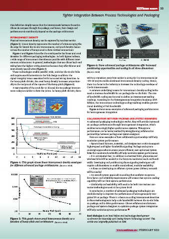
wiring have the highest wiring densities because they offer thinner and Figure 6: Some advanced package architectures offer increased
more closely spaced wires (Figure 4). partitioning opportunities and scaling in all three dimensions.
These technologies enable parallel, wide, and slow die-to-die links (Source: Intel)
and require careful attention to the link design to address the
signal-integrity issues associated with increased wiring densities. As will be a transition away from solder to using Cu-Cu interconnects (at
the bump pitch shrinks, the areal bump density increases proportion- ~20–25 μm) to enable continued interconnect density scaling. Hence,
ally to the reciprocal of the square of the bump pitch (Figure 5). there is a focus in the industry to increase the technology envelope of
A vast majority of the areal die-to-die and die-to-package intercon- Cu-Cu interconnects.
nects today use solder to form the joints. As bump pitch shrinks, there A common underlying reason for interconnect density scaling is the
need to increase bandwidth for on-package die-to-die links. The rate
of bandwidth scaling can be used to define an interconnect scaling
roadmap. According to the Heterogeneous Integration Roadmap 2019
Edition, the interconnect technology scaling roadmap enables genera-
tional doubling of link bandwidth.
Figure 6 shows some examples of advanced packaging architectures
for heterogeneous integration.
COLLABORATION BETWEEN PACKAGE AND SYSTEM DESIGNERS
As advanced packaging technologies evolve, they will provide increased
on-package performance through heterogeneous integration, which
enables increasingly higher-performance systems. This system
performance can be better realized by strengthening collaborative
partnerships between package and system designers.
Here are some examples of how collaborative partnerships will help
maximize system performance:
• System board features, materials, and designs must evolve to support
higher-speed and higher-bandwidth signaling. Package and system
co-design approaches to create power-efficient, cost-optimized system
links that maximize bandwidth will help maximize system performance.
• It is anticipated that, in addition to electrical links, photonics and
wireless links will be needed in the future to maximize reach and band-
Figure 4: This graph shows linear interconnect density envelopes width. Developing and proliferating those signaling techniques will
for different advanced package architectures. (Source: Intel) require collaborations to enable standardized, modular scalability.
• A focus on developing an efficient system power delivery network
will be needed.
• An overall system approach to cooling that conforms to system
form factor and reliability requirements will ensure that system cooling
capability will not limit system performance.
• Modularity and scalability will need to be built into various con-
nector technologies used at the system level.
In conclusion, a number of advanced packaging technologies are
available today to improve the performance of heterogeneously inte-
grated IP on package. There is a focus on scaling interconnect densities
in these technologies to help scale bandwidth between die-to-die links
on package and to drive performance. Closer collaborations between
package and system designers to optimize package system integration
will help maximize system performance. ■
Ravi Mahajan is an Intel Fellow and technology development
Figure 5: This graph shows areal interconnect density as a co-director for Assembly and Testing Future Technology at Intel. This
function of bump pitch and architecture. (Source: Intel) article was originally published on EDN.
www.eetimes.eu | FEBRUARY 2021