
Page 56 - EETEurope FlipBook February
P. 56
56 EE|Times EUROPE
Five Keys to Next-Generation IC Packaging Design
design is also a significant challenge to
first-time–right success. Heterogeneous
multi-substrate packages exhibit multiple
chip-package interactions. One of the
largest is thermal dissipation, especially of
the non-linearly generated heat typical in
such packages.
The digital-twin methodology enables multi-domain and cross-domain integration. A typical approach to thermal manage-
(Source: Mentor Graphics) ment uses a heat spreader for heat transfer
and dissipation. But a heat spreader is
this is done using industry-standard formats such as LEF/DEF, AIF, only as good as its design. For the heat spreader to be efficient and
GDS, or CSV/TXT files. Functionality should also exist in a way that effective, it must be designed and simulated in conjunction with the
automatically recognizes device and substrate interfaces without hav- package, not as an afterthought. Designing the entire package in
ing to instantiate pseudo-components. This allows for multi-designer 3D ensures efficacious heat-transfer realization without significant
asynchronous design and verification. That, in turn, ensures overall design compromises.
system success when all components are completed and integrated. Both 2.5D and 3D stacking can create a variety of unintentional
A primary benefit of the digital-twin approach is that it serves physical stresses, such as substrate warpage during mounting and
as the golden reference to drive complete physical and electrical bump-induced stress. Designers must be able to analyze a layout for
verification at every level of the design hierarchy. That eliminates the stresses caused by such chip-package interactions and their impact
multiple, static spreadsheets typically used to represent pin and con- on device performance. Once the package is nearing implemen-
nectivity information, replacing them with a full, system-level netlist tation completion, the accurate 3D packaging thermal model can
in Verilog format. be exported for inclusion in detailed PCB and full-system thermal
analysis. This enables final tuning of the system enclosure and allows
natural and/or forced cooling to be optimized.
Advanced IC packages bring many new challenges for signal integ-
rity engineers and their design tools. Dies are mounted directly to
the substrate, so it becomes possible to couple substrate routing with
on-die redistribution layer routing.
Packages are no longer simple, planar layer structures with easily
modeled, simple vias between metal layers. Instead, there can be mul-
tiple substrates of very different materials and properties. Analysis
can be used successfully for a number of signal- and power-integrity–
related items.
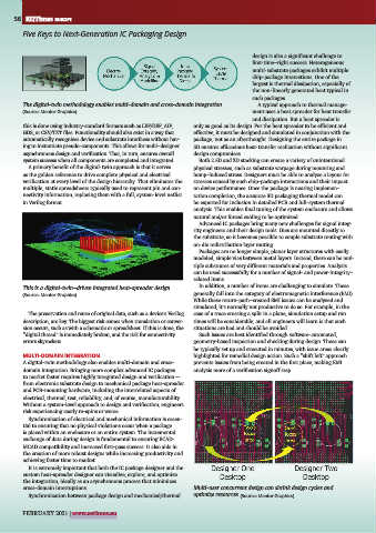
This is a digital-twin–driven integrated heat-spreader design. In addition, a number of items are challenging to simulate. These
(Source: Mentor Graphics) generally fall into the category of electromagnetic interference (EMI).
While these return-path–created EMI issues can be analyzed and
simulated, it’s normally not productive to do so. For example, in the
The preservation and reuse of original data, such as a device’s Verilog case of a trace crossing a split in a plane, simulation setup and run
description, are key. The biggest risk comes when translation or conver- times will be considerable, and all engineers will learn is that such
sion occurs, such as with a schematic or spreadsheet. If this is done, the situations are bad and should be avoided.
“digital thread” is immediately broken, and the risk for connectivity Such issues are best identified through software-automated,
errors skyrockets. geometry-based inspection and checking during design. These can
be typically set up and executed in minutes, with issue areas clearly
MULTI-DOMAIN INTEGRATION highlighted for remedial design action. Such a “shift left” approach
A digital-twin methodology also enables multi-domain and cross- prevents issues from being created in the first place, making EMI
domain integration. Bringing more complex advanced IC packages analysis more of a verification signoff step.
to market faster requires highly integrated design and verification —
from electronic substrate design to mechanical package heat-spreader
and PCB-mounting hardware, including the interrelated aspects of
electrical, thermal, test, reliability, and, of course, manufacturability.
Without a system-level approach to design and verification, engineers
risk experiencing costly re-spins or worse.
Synchronization of electrical and mechanical information is essen-
tial to ensuring that no physical violations occur when a package
is placed within an enclosure or an entire system. The incremental
exchange of data during design is fundamental to ensuring ECAD-
MCAD compatibility and increased first-pass success. It also aids in
the creation of more robust designs while increasing productivity and
achieving faster time to market.
It is extremely important that both the IC package designer and the
custom heat-spreader designer can visualize, explore, and optimize
the integration, ideally as an asynchronous process that minimizes
cross-domain interruptions. Multi-user concurrent design can shrink design cycles and
Synchronization between package design and mechanical/thermal optimize resources. (Source: Mentor Graphics)
FEBRUARY 2021 | www.eetimes.eu