
Page 51 - EETEurope FlipBook February
P. 51
EE|Times EUROPE 51
Heterogeneous Integration and the Evolution of IC Packaging
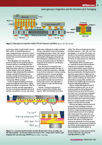
Figure 2: Heterogeneous integration exhibits TSV and interposer capabilities. (Source: Veeco Instruments)
performing at FEOL standards while running which create challenges for overlay and depth critical. The ability to handle warped wafers,
BEOL wafers. All photolithography pro- of focus, respectively, in advanced packaging broadband exposure — GHI-, GH-, and I-line
cesses emphasize feature resolution, critical photolithography process flows. This is where wavelengths — for multiple film stacks, and
dimension (CD) control, and overlay accuracy a different lithography approach is required, variable NA for resolution adaptability with
metrics while maintaining high productivity utilizing BEOL lithography tooling that has large depth of focus control have all proved
and low cost. been developed to address these issues with paramount for high productivity, high yield,
FEOL lithography tools that typically practical yet versatile solutions. The BEOL is and good cost of ownership.
operate at a high numerical aperture (NA) for recognized as the domain for metallization This flexibility will be extremely import-
resolution reasons are now tasked with fine and interconnects. ant, especially at outsourced semiconductor
line/space, via, and micro-bump patterning for Next, flip-chip (C4) bumping is a well- assembly and test facilities. Versatility to
initial interconnect definition. As interconnect defined and stable process that has been an match a variety of FEOL exposure field sizes,
and RDL density increases, the challenges industry standard for several years. Although substrate sizes, and material types is also an
relating to thicker photoresist films, substrate it, too, has been subjected to scaling, bumping important consideration. The requirements for
warpage, and depth of focus become com- is still fundamental to advanced packaging improved stage precision for tighter overlay,
pounded, and high-NA lithography systems for heterogeneous integration. Generally, higher throughput for greater productivity, and
frequenting the FEOL are no longer capable of bump lithography is performed with thicker tighter exposure uniformity for improved CD
running these difficult processes. photosensitive materials that benefit from uniformity are merging FEOL and BEOL tool
Certain advanced packaging technologies tooling with a low NA and a high depth of performance for leading-edge, heterogeneous
employ more difficult process flows, making focus to define the larger flip-chip bumps — integration technology applications.
wafers more difficult to manufacture. Take, for C4 technology. Modern, leading-edge applications such
instance, die shift and wafer topography on However, as industry segmentation as artificial intelligence, HPC, 5G, IoT, and
TSV-less reconstituted embedded wafer-level shrinks, drawing FEOL and BEOL closer consumer mobile are driving demand for
ball grid array (eWLB) or fan-out–type wafers, together, BEOL tool flexibility has become increased electronic device performance at
ever-lower costs. Heterogeneous integration
technology enables semiconductor device
manufacturers to combine functional compo-
nents from different manufacturing process
flows into a single composite device with
complex and advanced functionality.
Advanced packaging production demands
created by these technologies challenge
lithography and complementary processes to
perform at a higher standard to support the
required interconnect and TSV processing
layer requirements. Here, device cost and
lower productivity or yield due to increased
complexity are the challenges that manu-
facturers will address. Initially, high-end
applications will benefit from heterogeneous
integration before advancements in yield and
process flow enable packaging devices to be
cost-competitive for wider markets. ■
Figure 3: A conceptual implementation of multi-die with micro-bump, Cu pillar, and Gareth Kenyon is a senior product engineer
flip-chip bumping — in this case, without the need for TSV — using Amkor’s silicon wafer at Veeco Instruments. This article was
integrated fan-out technology (SWIFT) (Source: Amkor Technology) originally published on EDN.
www.eetimes.eu | FEBRUARY 2021