
Page 11 - PEN eBook February 2024
P. 11
SEMICONDUCTORS SEMICONDUCTORS
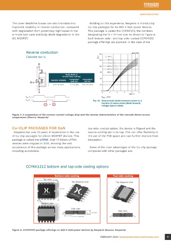
The lower deadtime losses can also translate into Building on this experience, Nexperia is introducing
improved reliability in reverse conduction, compared Cu-clip packages for its 650-V GaN power devices.
with degradation from potentially high losses in the This package is called the CCPAK1212, the numbers
e-mode GaN case and body diode degradation in the designating the 12 × 12-mm size. As shown in Figure 4,
SiC MOSFET. both bottom-side– and top-side–cooled CCPAK1212
package offerings are planned. In the case of the
Figure 1: Cascode architecture with the d-mode GaN power HEMT and some of its advantages (Source: Nexperia)
arrangement with the d-mode devices is its improved efficiency. The characteristics of the cascode device
performance at higher temperatures. As shown in make it more forgiving in the use of simpler bootstrap
Figure 2, e-mode devices (shown under the competitor gate drivers.
heading) show a fall in drain current of over 100%
from 25°C to 150°C, while the cascode devices show a Another key advantage of the d-mode cascode
smaller change at high temperatures. architecture is the much lower third-quadrant voltage Figure 3: A comparison of the reverse-current voltage drop and the reverse characteristics of the cascode device across
temperature (Source: Nexperia)
Cu-CLIP PACKAGES FOR GaN top-side–cooled option, the device is flipped and the
Nexperia has over 20 years of experience in the use source-cooling tab is on top. This can offer flexibility in
of Cu-clip packages for silicon MOSFET devices. This the use of the PCB space and can further improve heat
package is called the LFPAK. Over 1.7 billion LFPAK dissipation.
devices were shipped in 2021, showing the vast
acceptance of this package across many applications, Some of the main advantages of the Cu-clip package
including automotive. compared with other packages are:
Figure 2: A comparison of the drain-current gate-voltage–transfer characteristics at room and high temperatures (Source:
Nexperia)
Silicon carbide MOSFETs, much like silicon MOSFETs, drop under reverse conduction, as shown in Figure 3.
exhibit zero-temperature crossing in their transfer This arises from the fact that the only significant
curves. While it is generally advantageous for thermal voltage drop is from the low-voltage silicon MOSFET
runaway reasons to operate with the maximum rating body diode. The lower voltage drop can increase the
on the negative drain-current temperature coefficient flexibility in the deadtime of the circuit (shown as
part of the curve, the cascode device characteristics times A and B in Figure 3) and lower deadtime loss
allow for the use of devices with less of a derating for a given deadtime. This loss can be exacerbated for
in the maximum high-temperature power ratings e-mode devices if a negative V is used at turn-off,
gs
compared with e-mode devices, leading to improved as is often the case due to the low V of the device. Figure 4: CCPAK1212 package offerings on 650-V GaN power devices by Nexperia (Source: Nexperia)
th
10 FEBRUARY 2024 | www.powerelectronicsnews.com FEBRUARY 2024 | www.powerelectronicsnews.com 11