
Page 12 - PEN eBook February 2024
P. 12
SEMICONDUCTORS SEMICONDUCTORS
Figure 6: Hard-switching 100-kHz, 400- to 230-V buck converter waveform and efficiency curve for the 650-V top-side–cooled
650-V GaN in the CCPAK package (Source: Nexperia)
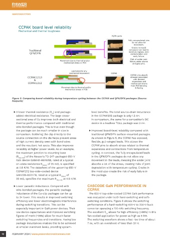
Figure 5: Comparing board reliability during temperature cycling between the CCPAK and QFN/DFN packages (Source:
Nexperia)
power-switching applications. GaN HEMTs, with their
low reverse-recovery losses, allow for the use of
▶ A lower thermal resistance (R ) and package- level benefits. The total source-drain inductance simpler topologies, such as the totem pole for the PFC
th
added electrical resistance. The large cross- in the CCPAK1212 package is only 1.2 nH. stage. The much higher switching frequencies with GaN
sectional area of Cu improves both electrical and In comparison, the same for a competitor’s SiC can result in improved power densities and reduced
thermal performance compared with traditional device in a leadless TOLL package was 2 nH. system cost with smaller magnetics.
wire-bonded packages. This is true even though
the package can be much smaller in size in ▶ Improved board-level reliability compared with An example application is a single-phase solar
comparison. Soldering the clip directly to the traditional QFN/DFN surface-mounted packages. inverter. A simplified block diagram of this is shown in
source connection on the die helps prevent areas As shown in Figure 5, the CCPAK has exposed, Figure 8. Half-bridge GaN devices can be used for the
of high current density seen with bond wires flexible, gull-winged leads. This allows the MPPT and DC/DC boost of the incoming PV voltage,
and the resultant hot spots. This also improves CCPAK pins to absorb stress related to thermal while the high-switching GaN devices in the inverter
reliability at higher power levels. As an example, expansions and contractions from temperature can reduce the size of the line filters and magnetics.
the maximum junction to mounting base cycling. In contrast, the fully encapsulated leads
(R th(j-mb) ) of the Nexperia TO-247–packaged 650-V in the QFN/DFN packages do not allow any
GaN device GAN041-650WSB, rated at a typical movement in the leads, meaning the solder joint Figure 7: Soft-switching 1-MHz converter switching loss
on-state resistance R DS(on) of 35 mΩ, is specified absorbs a lot of the stress, creating risks of joint comparisons (Source: Nexperia)
at 0.8 K/W. The datasheet of the upcoming 650-V degradation with temperature cycling. Cracks in
CCPAK1212 top-side–cooled device the mold also create the risk of early failure in The switching loss comparison of a resonant soft-
GAN039-650NTB, rated at a typical R DS(on) of the package. switching converter at a 400-V DC bus voltage and
33 mΩ, specifies the maximum R th(j-mb) at 0.5 K/W. switching at 1 MHz is shown in Figure 7. The CCPAK
GaN device is a lower R DS(on) compared with the rest of
▶ Lower parasitic inductance. Compared with CASCODE GaN PERFORMANCE IN the devices shown in Figure 7 and would hence exhibit
wire-bonded packages, the parasitic package CCPAK greater parasitic switching losses for the same FOM.
inductance of the Cu-clip packages can be up The 650-V top-side–cooled CCPAK GaN performance However, the clear FOM advantages of GaN, as well as
to 3× lower. This results in improved switching was evaluated under both hard-switching and soft- the cascode and CCPAK package advantages, result in
efficiency and lower electromagnetic interference switching conditions. Figure 6 shows the switching a much lower switching loss for this device compared
during switching transitions. This can be performance of a hard-switching 400-V to 230-V buck with the silicon, SiC and e-mode GaN devices.
especially important in GaN power devices. Their converter operating a 100-kHz switching frequency.
low device capacitances and improved switching The excellent R allows for high efficiency (>98%) in this The cascode architecture and the CCPAK package
th
figures of merit (FOMs) allow for much faster fan-cooled application for power as high as 6 kW. together serve some of GaN’s inherent benefits to a
switching frequencies and transitions. Having low The switching waveform shows a fast rise time of about greater extent. The new 33-mΩ 650-V GaN FETs from
package inductances enables this to be achieved 7 ns, with an overshoot of less than 20 V. Nexperia, offered in a top-side– and bottom-side– Figure 8: A simplified block diagram of a single-phase solar
inverter showing the use of GaN in the DC/DC boost stage, as
at smaller overshoot levels, providing system- cooled CCPAK package, provide many advantages in well as the inverter (Source: Nexperia)
12 FEBRUARY 2024 | www.powerelectronicsnews.com FEBRUARY 2024 | www.powerelectronicsnews.com 13