Page 6 - PEN eBook February 2024
P. 6

COVER STORY – DESIGN                                                                                                                                                                                        COVER STORY – DESIGN

                                                                                                                                 devices. The significance of these tests lies in their   dynamic negative and positive voltages. The company
                                                                                                                                 capacity to detect and rectify potential flaws and   has created exclusive and patented techniques to
                                                                                                                                 malfunctions in semiconductor devices before        ensure that all the thousands of dies on GaN and SiC
                                                                                                                                 their packaging and delivery to customers. By doing   wafers remain in complete contact while preventing
                                                                                                                                 these tests at the wafer stage, manufacturers can   arcing in high-voltage situations, especially in
                                                                                                                                 identify and resolve problems at an early stage of   fine-pitch geometries.
                                                                                                                                 manufacturing, hence minimizing the likelihood of
                                                                                                                                 defective devices being released to the market.

                                                                                                                                  At the forefront of this technology is Aehr Test
                                                                                                                                 Systems, a global supplier of test equipment used
                                                                                                                                 for the process of burning in and testing integrated
                                                                                                                                 circuits that are used in logic, optoelectronic and
                                                                                                                                 memory applications. Headquartered in Fremont,
                                                                                                                                 California, the company offers a wide portfolio
                                                                                                                                 of products used for testing and burning in
                                                                                                                                 semiconductor devices at various stages, including
                                                                                                                                 wafer level, singulated die and package part form.

                                                                                                                                  In an interview with Power Electronics News,
                                                                                                                                 Vernon Rogers, EVP of sales and marketing at Aehr
                                                                                                                                 Test Systems, provided insights on these innovative
                                                                                                                                 testing methodologies, explaining how they can
                                                                                                                                 assess the quality and reliability of semiconductors,
                                                                                                                                 including emerging WBG materials like GaN and
          Wafer-Level Test and                                                                                                   silicon carbide.

                                                                                                                                 WBG TESTING SOLUTIONS
          Burn-In Advances GaN                                                                                                   and frontrunner in the burn-in and semiconductor
                                                                                                                                  Aehr Test Systems is acknowledged as a trailblazer
                                                                                                                                 test sector, possessing a patent portfolio that
          Reliability                                                                                                            encompasses groundbreaking ideas in fields like
                                                                                                                                 portable WaferPaks and exceptionally parallel testing
                                                                                                                                 capabilities. Recently, the company received an initial
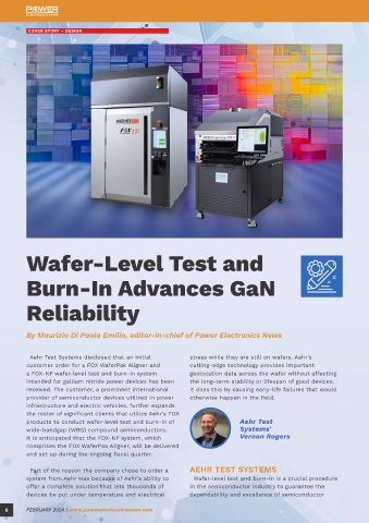
                                                                                                                                 customer order for a FOX-NP wafer-level test and    Figure 1: Aehr’s FOX-NP system (Source: Aehr Test Systems)
          By Maurizio Di Paolo Emilio, editor-in-chief of Power Electronics News                                                 burn-in system (Figure 1) and a FOX WaferPak Aligner
                                                                                                                                 intended for GaN power devices.
                                                                                                                                                                                      Wafer-level burn-in is a crucial step in WBG
           Aehr Test Systems disclosed that an initial        stress while they are still on wafers. Aehr’s                       “Our FOX systems employ an innovative combination   semiconductor manufacturing. It involves subjecting
          customer order for a FOX WaferPak Aligner and       cutting-edge technology provides important                         of thermal control mechanisms and electrical stress   the wafers to elevated temperatures and electrical
          a FOX-NP wafer-level test and burn-in system        geolocation data across the wafer without affecting                conditions to perform wafer-level burn-in testing on   stresses for a specified period, as defined by the
          intended for gallium nitride power devices has been   the long-term stability or lifespan of good devices.             gallium nitride, along with silicon carbide and other   customer’s high-temperature gate bias,
          received. The customer, a prominent international   It does this by causing early-life failures that would             devices,” Rogers said.                              high-temperature reverse bias, time-dependent
          provider of semiconductor devices utilized in power   otherwise happen in the field.                                                                                       dielectric breakdown, threshold voltage and other
          infrastructure and electric vehicles, further expands                                                                   Aehr’s unique compact system architecture          test specifications.
          the roster of significant clients that utilize Aehr’s FOX                                                              supports full wafer test and thermal control and
          products to conduct wafer-level test and burn-in of                 Aehr Test                                          wafer handling in a form factor called a “Blade,”    “Subjecting each wafer to accelerated stress
          wide-bandgap (WBG) compound semiconductors.                         Systems’                                           in either a 3.4-inch (8.5-cm) height test for higher   conditions, such as elevated temperatures and
          It is anticipated that the FOX-NP system, which                     Vernon Rogers                                      parallelism or a 6.8-inch (17.2-cm) height test     increased voltage levels, help uncover latent defects
          comprises the FOX WaferPak Aligner, will be delivered                                                                  for more channels. The FOX platform features a      or weaknesses in the devices that might lead to
          and set up during the ongoing fiscal quarter.                                                                          sophisticated thermal control system that offers    early-life failures,” Rogers said.
                                                                                                                                 precise cold and hot thermal control to each
           Part of the reason the company chose to order a    AEHR TEST SYSTEMS                                                  wafer. This is achieved by applying electrical stress   “The challenge with test and burn-in is to not
          system from Aehr was because of Aehr’s ability to    Wafer-level test and burn-in is a crucial procedure               conditions to each wafer using Aehr’s exclusive     exceed the device limitations that can actually
          offer a complete solution that lets thousands of    in the semiconductor industry to guarantee the                     precision power supplies and measurement            create latent defects, or ‘walking wounded,’ devices,
          devices be put under temperature and electrical     dependability and excellence of semiconductor                      instruments, which can generate a wide range of     and this requires a careful balancing of electrical,

   6      FEBRUARY 2024 | www.powerelectronicsnews.com                                                                                                                                        FEBRUARY 2024 | www.powerelectronicsnews.com   7
   1   2   3   4   5   6   7   8   9   10   11