
Page 46 - PEN eBook May 2023
P. 46
: DESIGN DESIGN
single SiC die and seven pins for the gate (G, one pin),
driver source (DS, one pin) and power source (PS, five
pins), the exposed lead frame is present at the back of
the package and connected to the drain terminal of the
SiC MOSFET.
The SCT040H65G3AG die features a vertical
planar-gate design with a pitch of 4.8 µm, planar
polysilicon gate and single thick pre-metal dielectric
deposited on the polysilicon to isolate the gate from
the source/body metal.
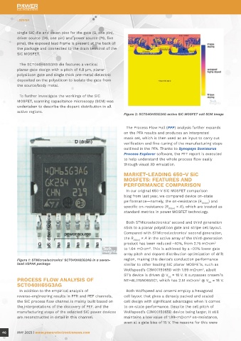
To further investigate the workings of the SiC
MOSFET, scanning capacitance microscopy (SCM) was Figure 3: Selected 3D emulation results at various stages of the STMicroelectronics SCT040H65G3AG flow — (a) right after P⁺
undertaken to describe the dopant distribution in all blocking lithography; (b) at the completion of P⁺ implant module; (c) just after top metal deposition
active regions.
Figure 2: SCT040H65G3AG active SiC MOSFET cell SCM image
discussed in our blog “Reviewing Approaches to SiC MOSFET was selected last year by TechInsights as
MOSFET Cell Design.” a candidate to offer a complete analysis, including
The Process Flow Full (PFF) analysis further expands SiC Power Floorplan, PEF, Process Flow Analysis
on the PFA results and produces an interpreted In vertical power SiC MOSFETs, trench-gate designs and PFF reports. For details of our complete Power
mask set, which is then used as an input to carry out can bring an on-state performance advantage, although Semiconductor subscription offerings, please see the
verification and fine-tuning of the manufacturing steps significant shielding is often needed to protect the Power Semiconductor Product Vertical Overview.
outlined in the PFA. Thanks to Synopsys Sentaurus trench regions, as also discussed previously. Given the
Process Explorer software, the PFF report is executed automotive applications of STMicroelectronics’ device, Four years after STMicroelectronics delivered its
to help understand the whole process flow easily it makes sense that ST has stuck with the somewhat- second-generation product, without a big change
through visual 3D emulation. conservative planar gate rather than trench to avoid in the device layout (still employing the scheme
any tricky issues with device robustness. of planar polysilicon gate and stripe cell layout), it
MARKET-LEADING 650-V SiC successfully elevated its third-generation
MOSFETS: FEATURES AND CONCLUSION 650-V product performance to compete with leading
PERFORMANCE COMPARISON The 650-V class of SiC MOSFETs is one of competitors by reducing the cell pitch and possibly
In our original 650-V SiC MOSFET comparison the hottest topics in the power semiconductor optimizing dopant distribution of the drift region.
blog from last year, we compared device on-state market, with potential applications spanning Coupling this with STMicroelectronics’ previous
performance—namely, the on-resistance (R DS(on) ) and many high-growth markets, not least automotive. success with automotive-grade SiC MOSFETs makes
specific on-resistance (R DS(on) × A), which are treated as STMicroelectronics’ automotive-grade this part a formidable entrant to the market.
standard metrics in power MOSFET technology. third-generation 650-V SCT040H65G3AG SiC
Both STMicroelectronics’ second and third generation
stick to a planar polysilicon gate and stripe cell layout.
Compared with STMicroelectronics’ second generation,
the R DS(on) × A in the active array of the third-generation
product has been reduced ~40%, from 2.75 mΩ·cm
2
to 1.64 mΩ·cm . This is achieved by a ~20% lower gate
2
array pitch and dopant distribution optimization of drift
Figure 1: STMicroelectronics’ SCT040H65G3AG in a seven- region, making this device’s conduction performance
lead H2PAK package similar to other leading SiC planar MOSFETs, such as
Wolfspeed’s C3M0015065D with 1.99 mΩ·cm , albeit
2
ST’s device is driven @ V = 18 V. It surpasses onsemi’s
GS
PROCESS FLOW ANALYSIS OF NTH4L015N065SC1, which has 2.51 mΩ·cm @ V = 18 V.
2
SCT040H65G3AG GS
In addition to the empirical analysis of Both Wolfspeed and onsemi employ a hexagonal
reverse-engineering results in PFR and PEF channels, cell layout that gives a densely packed and scaled
the SiC process flow channel is mainly built based on cell design with significant advantages when it comes
the interpretations of the discovery of PEF, and the to on-state performance. Despite the cell pitch of
manufacturing steps of the selected SiC power devices Wolfspeed’s C3M0015065D device being larger, it still
are reconstructed in detail in this channel. maintains a low value of 1.99-mΩ·cm2 on-resistance,
even at a gate bias of 15 V. The reasons for this were
46 MAY 2023 | www.powerelectronicsnews.com MAY 2023 | www.powerelectronicsnews.com 47