
Page 45 - PEN eBook May 2023
P. 45
SEMICONDUCTORS DESIGN
The Cu clip also lowers package inductance, which The main features of this latest innovative package
is 3× lower than traditional wire-bonded packages, can be summarized as follows:
allowing for higher switching efficiency and less
electromagnetic interference (EMI). In today’s power ▶ Small form factor (12 × 12 mm) and low
supply designs, which aim for higher frequencies to package height (2.5 mm) compared with
provide greater power density and faster dynamic traditional through-hole packaging like TO-247
response, boosting switching efficiency is becoming
increasingly crucial. ▶ Wire-bond–free for low inductances and
ultra-low package resistance; Cu clip offers
CCPAK ADDS SUPPORT FOR WBG 3× lower inductances than industry-standard
SEMICONDUCTORS packages for lower switching losses and EMI
The natural evolution of LFPAK technology is CCPAK,
developed to boost the power handling, electrical ▶ Flexible gull-wing leads that offer higher
efficiency and reliability capabilities offered by the board-level reliability and easy optical
incoming generation of wide-bandgap (WBG) devices. inspection that gives compatibility with SMD
soldering and automatic optical inspection
▶ Excellent thermal performance with thermal
resistance of typically less than 0.5 K/W,
providing optimal cooling and operating with a
maximum temperature of 175°C
▶ Two cooling options available: bottom-side
cooling (CCPAK1212) and top-side cooling A Deep Dive into ST’s
(CCPAK1212i)
CCPAK1212 is an ideal package for Nexperia’s Third-Gen
GaN-based power transistors. GaN and Cu clip
are a great match, as WBG technology can provide
outstanding efficiency in fast-switching circuits, Automotive-Grade SiC
meeting even the most demanding requirements
coming from the automotive industry.
Nexperia shipped over 1.7 billion pieces in 2021 and MOSFETs
Figure 2: A CCPAK1212 GaN FET power device (Source: another 1.9 billion pieces in 2022 (LFPAK devices,
Nexperia) including MOSFETs and bipolar power transistors By Deyan Chen and Stephen Russell, subject matter experts at TechInsights
in the LFPAK56 and its later versions, which ranged
The Cu-clip technology from Nexperia has in size from the smaller 3 × 3-mm LFPAK33 to the
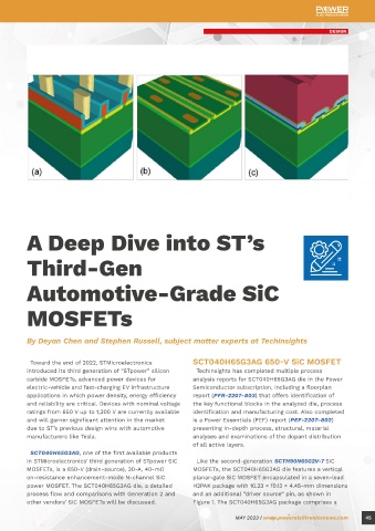
revolutionized the power packaging industry and has larger 8 × 8-mm LFPAK88). With the addition of the Toward the end of 2022, STMicroelectronics SCT040H65G3AG 650-V SiC MOSFET
set the standard for performance and efficiency ever new CCPAK1212 to the Cu-clip product portfolio, introduced its third generation of “STpower” silicon TechInsights has completed multiple process
since. With the introduction of Cu clip in 2002, over Nexperia believes this technology will continue carbide MOSFETs, advanced power devices for analysis reports for SCT040H65G3AG die in the Power
90% of Nexperia’s product line now utilizes the LFPAK to play a significant role in cutting-edge power electric-vehicle and fast-charging EV infrastructure Semiconductor subscription, including a floorplan
loss-free package. This technology is prominent in semiconductors for many years, whether employing applications in which power density, energy efficiency report (PFR-2207-803) that offers identification of
the new CCPAK1212, shown in Figure 2, which houses GaN or SiC or MOSFET devices. and reliability are critical. Devices with nominal voltage the key functional blocks in the analyzed die, process
Nexperia’s most recent GaN FETs. ratings from 650 V up to 1,200 V are currently available identification and manufacturing cost. Also completed
and will garner significant attention in the market is a Power Essentials (PEF) report (PEF-2207-802)
due to ST’s previous design wins with automotive presenting in-depth process, structural, material
manufacturers like Tesla. analyses and examinations of the dopant distribution
of all active layers.
SCT040H65G3AG, one of the first available products
in STMicroelectronics’ third generation of STpower SiC Like the second-generation SCTH90N65G2V-7 SiC
Reference MOSFETs, is a 650-V (drain-source), 30-A, 40-mΩ MOSFETs, the SCT040H65G3AG die features a vertical
on-resistance enhancement-mode N-channel SiC planar-gate SiC MOSFET encapsulated in a seven-lead
power MOSFET. The SCT040H65G3AG die, a detailed H2PAK package with 10.23 × 10.13 × 4.45-mm dimensions
▶ 1Yandoc, D. (Dec. 16, 2022). “How Copper Clip Makes Perfect Packages for the Future of Power.” Blog post. process flow and comparisons with Generation 2 and and an additional “driver source” pin, as shown in
other vendors’ SiC MOSFETs will be discussed. Figure 1. The SCT040H65G3AG package comprises a
44 MAY 2023 | www.powerelectronicsnews.com MAY 2023 | www.powerelectronicsnews.com 45