Page 42 - PEN eBook May 2023
P. 42

SEMICONDUCTORS                                                                                                                                                                                                  SEMICONDUCTORS

                                                                                                                                  Compared with D2PAK technology, based on wire      exponentially more transistors while reducing the
                                                                                                                                 bond, LFPAK offers the following benefits:          supply voltage. Because the standard SO-8 transistor
                                                                                                                                                                                     package couldn’t handle it all, power supply designs
                                                                                                                                  ▶  Prevents localized current crowding             had to become more complex, using larger packages
                                                                                                                                                                                     like DPAK and even D2PAK.
                                                                                                                                  ▶  Allows for a more uniform current spread
                                                                                                                                                                                      To replace DPAK or D2PAK, LFPAK56 was developed
                                                                                                                                  ▶  Acts as a heatsink to the die                   to provide greater power from the widespread SO-8
                                                                                                                                                                                     package footprint. Despite having less than half the
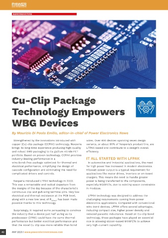
                                                                                                                                  The internal structure of an LFPAK MOSFET is       footprint size (LFPAK’s 30 mm2, compared with DPAK’s
                                                                                                                                 shown in Figure 1. Cu clips can withstand very      70 mm2), the initial generation of 25-V MOSFETs in
                                                                                                                                 high temperatures, as the melting temperature of    LFPAK56 (which owes its name to its size of 5 × 6 mm)
                                                                                                                                 copper is about 900°C. The silicon die, due to the   exhibited R DS(on)  and maximum drain current equivalent
                                                                                                                                 doping process, can operate up to 250°C without     to identical devices in DPAK. Because of its enormous
                                                                                                                                 compromising the switching performance. The plastic   cross-sectional area, the Cu-clip attachment, which
                                                                                                                                 mold compound, whose composition is carefully       substitutes conventional bond-wire connections
                                                                                                                                 selected to withstand high-temperature specification,   between the die and leadframe, significantly improves
                                                                                                                                 can potentially harden and becomes brittle at about   electrical and thermal performance.
                                                                                                                                 190°C and above. As a result, the internal components
                                                                                                                                 of the MOSFET are either naturally capable of        How LFPAK56, at less than half the size of DPAK,
          Cu-Clip Package                                                                                                        withstanding temperatures >175°C or specifically    could achieve equal thermal performance baffled the
                                                                                                                                 selected to do so.
                                                                                                                                                                                     industry at first. Although the physics of soldering the
                                                                                                                                                                                     clip directly to the source connection on the device
          Technology Empowers                                                                                                    limited to 175°C due to the reliability standards that   eliminated the high-current–density regions that often
                                                                                                                                  The maximum junction temperature of MOSFETs is
                                                                                                                                                                                     exist where bond wires are joined, others questioned
                                                                                                                                 MOSFETs must adhere to. By industry standards,
                                                                                                                                                                                     the clip attachment’s reliability. Consequently, a Cu clip
          WBG Devices                                                                                                            Nexperia uses a temperature limit of 175°C for MOSFET   shields the transistor by preventing the development of
                                                                                                                                 qualification and life testing.
                                                                                                                                                                                     thermal “hotspots” at specific sites.


          By Maurizio Di Paolo Emilio, editor-in-chief of Power Electronics News

           Strengthened by the innovations introduced with    wires. Over 400 devices spanning seven design
          copper (Cu)-clip package (CCPAK) technology, Nexperia   variants, or about 90% of Nexperia’s product line, are
          brings its long-time experience producing high-quality   LFPAK-based and contribute to a design’s overall
          and robust SMD packaging to its gallium nitride FET   efficiency.
          portfolio. Based on proven technology, CCPAK provides
          industry-leading performance in a                   IT ALL STARTED WITH LFPAK
          wire-bond–free package optimized for thermal and     In automotive and industrial applications, the need
          electrical performance, simplifying the design of   for high power has increased in modern electronics.
          cascode configuration and eliminating the need for   Kilowatt power output is a typical requirement for
          complicated drivers and controls.                   applications like motor drives, inverters or on-board
                                                              chargers. This means the need to handle greater
           Nexperia introduced LFPAK technology in 2002.      power is being transferred to the components,
          This was a remarkable and radical departure from    especially MOSFETs, due to existing space constraints
          the designs of the day because of the characteristic   in modules.
          continuous clip and gull-wing terminal pins. Very low
          electrical and thermal resistance at the PCB level,   LFPAK technology was designed to address the                     Figure 1: LFPAK internal structure (Source: Nexperia)
          along with a new low level of R DS(on) , has been made   challenging requirements coming from power
          possible thanks to this technology.                 electronics applications. Compared with conventional
                                                              wire-bond devices, LFPAK offers several advantages,                 The computing industry requires exceptionally       Testing for reliability and thermal performance
           Surprisingly, it required some persuading to convince   including compact size, higher power density and              high current to power the newest generation of      demonstrated that LFPAK could deliver on its
          the industry that a device just half as big as its   reduced parasitic inductance. Based on Cu-clip bond               processors and microcontrollers, which is why       promises. Moreover, LFPAK56 passed the demanding
          predecessor (DPAK) could have the same thermal      technology, these packages have played an essential                Nexperia created LFPAK technology. The peak         2× AEC-Q101 automotive qualification, exceeding all
          performance but better electrical performance and   role in allowing silicon-based MOSFETs to achieve                  current started approaching 200 A and beyond as     standards by a wide margin.
          that the novel Cu clip was more reliable than bond   very high-current capability.                                     each new silicon technology node brought on-chip

  42      MAY 2023 | www.powerelectronicsnews.com                                                                                                                                                  MAY 2023 | www.powerelectronicsnews.com  43
   37   38   39   40   41   42   43   44   45   46   47