
Page 23 - PEN eBook May 2022
P. 23
DESIGN Design
THERMAL MANAGEMENT OF POWER DEVICES
The power-electronic market requires increasingly smaller, more efficient, and more reliable
devices. Key factors to meet these stringent requirements are a high power density (able to reduce
both the footprint and the costs of the solution) and excellent thermal management (able to keep
the device temperatures under control). The three main requirements of a thermal management
system for power semiconductors are the following:
1. Heat shall be conducted from the device to the ambient environment with a thermal
resistance low enough to prevent the junction temperature (T ) from increasing beyond a
J
specified limit. Due to the derating factor, T is usually lower than the datasheet value.
J
2. Electrical isolation between the power circuit and the ambient environment shall be provided.
3. Thermally induced mechanical stress resulting from material coefficient of thermal expansion
mismatch shall be absorbed.
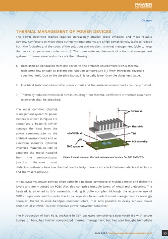
The most common thermal
Simple and management system for power
devices is shown in Figure 1. It
comprises a heatsink (which
Performant Thermal conveys the heat from the
power semiconductor to the
Management Solution ambient environment) and an
electrical insulator (thermal
for CSP GaN FETs interface material, or TIM) to Figure 1: Most common thermal management system for CSP GaN FETs
separate the metal heatsink
from
the
semiconductor
junction. Because most
By Stefano Lovati, technical writer for EEWeb
dielectric materials have low thermal conductivity, there is a tradeoff between electrical isolation
and thermal resistance.
Thanks to a better figure of merit, wide-bandgap semiconductors such as gallium nitride offer a
1
higher power density than silicon, occupying less area on the die and therefore requiring a package In real systems, power devices often come in a package composed of multiple metal and dielectric
with smaller size. Assuming that the area occupied by the device is the main factor that determines layers and are mounted on PCBs that also comprise multiple layers of metal and dielectrics. The
thermal performance, it is reasonable to assume that a smaller power device leads to higher heatsink is attached to this assembly, making it quite complex. Although the extensive use of
thermal resistance. This article will demonstrate how chip-scale–packaging (CSP) GaN FETs offer SMD components and the reduction in package size have made thermal management increasingly
3,4
thermal performance at least equal to, if not superior to, that of silicon MOSFETs. Due to their complex, thanks to wide-bandgap semiconductors, it is now possible to easily achieve power
superior electrical performance, the size of GaN FETs can be reduced, increasing the power density densities of 2 kW/in. in cost-effective power-converter solutions. 5
3
while respecting temperature limits. This behavior will be shown through detailed 3D finite element
simulations of the PCB layout while also providing experimental verification to support the analysis. The introduction of GaN FETs, available in CSP packages comprising a passivated die with solder
Read the original article here. 2 bumps or bars, has further complicated thermal management but has also brought immediate
32 MAY 2022 | www.powerelectronicsnews.com MAY 2022 | www.powerelectronicsnews.com 33