
Page 17 - Power Electronics News - December 2020
P. 17
Test & Measurements Test & Measurements
SiC promises lighter-weight components for risk than ‘tried and true’ Si-based power sem- and the time spent in the off state. For obvious in critical applications such as those related to
lower fuel consumption and lower emissions for iconductors. Therefore, there are several chal- reasons, unless this phenomenon is suppressed renewable energy. A significant amount of in-
the aerospace industry. This material facilitates lenges for GaN-based product designers. or understood then it is not possible to design vestment is being made by the industry to better
higher switching and higher power density for reliable circuits using GaN devices. evaluate the capability of GaN power devices to
a given voltage and current rating in a smaller, meet the needs of multiple power applications.
lighter device. CHARACTERIZATION OF GAN Within the last few years, JEDEC created a new
DEVICES workgroup (JC-70) to develop appropriate stand-
GaN, like silicon, can be used to create semicon- GaN device characterization presents some ards for WBG power semiconductors, in particu-
ductor devices such as diodes and transistors. A challenges that are common to all wide band gap lar GaN and SiC. The subgroups with JC-70 are
power supply designer could choose a GaN tran- (WBG) devices and some that are specific to GaN. focused on : 1) reliability, 2) datasheets, and 3)
sistor over a silicon one for its small form factor The common challenges are: test methods and characterization.
and high efficiency. GaN transistors also dissipate
less power and offer higher thermal conductivity, ▶ Data sheets are often insufficient to accu- Power Electronics News: What are the differenc-
compared to silicon devices with higher thermal rately represent the needed operating perfor- es of T&M compared with Silicon? Please provide
management requirements. GaN transistors are mance of the devices. one example.
increasingly used in various fields: in the auto-
motive sector, for the supply of electrical power, ▶ The need to accurately characterize very Mike Hawes: One key difference between Si and
and for the conversion and use of current. These small on-resistance under normal operating WBG devices (especially GaN) is switching speed.
components will soon replace their respective conditions (which are at hundreds of amps A GaN device typically switches 10 to 100 times
predecessors. and thousands of volts). faster than a comparable silicon transistor. The
switching frequency of a GaN device operating
In an interview with Power Electronics News, ▶ The need to accurately characterize device in a power conversion circuit is itself not fast
Alan Wadsworth - business development manag- capacitance under thousands of volts of enough to create issues, but higher-frequency
er for Keysight Technologies’ precision and pow- drain to source bias. components in the switching waveform can cre-
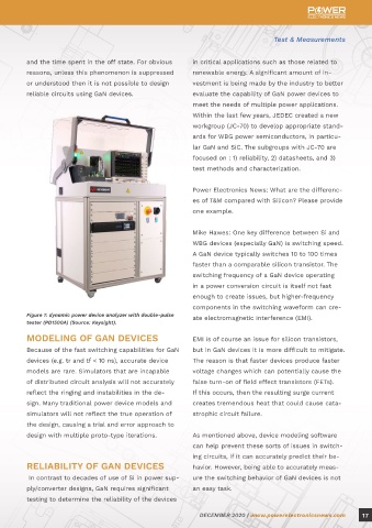
er products and Mike Hawes – Keysight’s Power Figure 1: dynamic power device analyzer with double-pulse ate electromagnetic interference (EMI).
tester (PD1500A) (Source: Keysight).
Solution Consultant, analyzed different aspects ▶ The need to measure gate charge character-
of Test&Measurements (T&M) for wide bandgap istics under a range of operating conditions MODELING OF GAN DEVICES EMI is of course an issue for silicon transistors,
solutions. (which again are at hundreds of amps and Because of the fast switching capabilities for GaN but in GaN devices it is more difficult to mitigate.
thousands of volts). devices (e.g. tr and tf < 10 ns), accurate device The reason is that faster devices produce faster
models are rare. Simulators that are incapable voltage changes which can potentially cause the
Power Electronics News: Power ▶ The need for dynamic characterization, includ- of distributed circuit analysis will not accurately false turn-on of field effect transistors (FETs).
semiconductor manufacturers believe ing conduction, drive, and switching losses. reflect the ringing and instabilities in the de- If this occurs, then the resulting surge current
that GaN-based devices hold the key sign. Many traditional power device models and creates tremendous heat that could cause cata-
to addressing a primary hurdle for the GaN devices also have some characteristics that simulators will not reflect the true operation of strophic circuit failure.
expansion of renewable energy. What are unique to them (and are not shared, for ex- the design, causing a trial and error approach to
are the challenges in terms of T&M to ample, with SiC devices). The unique feature of design with multiple proto-type iterations. As mentioned above, device modeling software
guarantee a good GaN-based product? GaN devices is that they can experience a phe- can help prevent these sorts of issues in switch-
Alan Wadsworth: GaN has some fundamental nomenon known as “current collapse”. This be- ing circuits, if it can accurately predict their be-
advantages over Si when being used in a switch havior causes the on-resistance of the transistor RELIABILITY OF GAN DEVICES havior. However, being able to accurately meas-
mode power converter (e.g. higher voltage, re- to change dynamically after turning on, with the In contrast to decades of use of Si in power sup- ure the switching behavior of GaN devices is not
duced losses, more compact, and faster switch- initial value of the on-resistance being depend- ply/converter designs, GaN requires significant an easy task.
ing). However, it is a newer technology with more ent on both the magnitude of the drain voltage testing to determine the reliability of the devices
16 DECEMBER 2020 | www.powerelectronicsnews.com DECEMBER 2020 | www.powerelectronicsnews.com 17