
Page 54 - EE Times Europe March 2022
P. 54
54 EE|Times EUROPE
SEMICONDUCTOR INDUSTRY
Unlocking the Potential of Molecular Beam
Epitaxy
By Anne-Françoise Pelé
nprecedented demand for more
powerful and energy-efficient
devices has spurred the need for
Ucompound semiconductors such as
gallium arsenide, gallium nitride, and silicon
carbide. Such materials require ultra-pure
thin films grown by epitaxy. Although molec-
ular beam epitaxy (MBE), one of three types of
epitaxy equipment, has long been considered
niche, it is poised to transition to volume
applications.
During a recent webinar, Riber, French
provider of MBE equipment serving the semi-
conductor industry, and Yole Développement,
French research and strategy consulting firm,
presented the current status and outlook of
the global MBE equipment market.
MOCVD, HTCVD, MBE
The epitaxy equipment market is segmented
by technology. Metal-organic chemical-
vapor deposition (MOCVD) epitaxy equip-
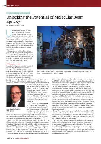
ment covers most of the III–V epitaxy, while Riber claims the MBE 8000 is the world’s largest MBE machine to produce VCSELs for
high-temperature CVD (HTCVD) is the most facial recognition and automotive LiDAR.
common deposition technique for silicon and
SiC devices. As Yole explains in a recently
published report, “Epitaxy Equipment for More Than Moore 2021,” enue of US$45 million in 2020, but will grow at a healthy 7.1% CAGR to
MOCVD is required for commodity devices such as GaN-based tradi- reach US$68 million in 2026. “This forecast is only for equipment and
tional LEDs. However, a growing number of high-end applications, such does not include services and spare parts, which represent a significant
as fast chargers, MicroLED displays, value of that market,” said Jean-Christophe Eloy, CEO of Yole.
and vertical-cavity surface-emitting MBE is often considered to be a niche technique and faces the
lasers (VCSELs) for 3D sensing, will unfortunate misconception that it is suitable only for research and
drive demand in the coming years. pilot production. For example, while it is true that Riber began in 1964
For HTCVDs, the primary market by supplying research laboratories and universities, it now has 750 MBE
is power applications, which are machines in operation in the world, and some leading semiconductor
based on silicon and SiC epi material foundries use MBE exclusively in their production environment.
and are mainly deployed in market Riber is at the start of the compound semiconductor value chain. It
segments such as automotive and delivers MBE systems for both research on compound semiconductor
industrial. materials and for volume production of epi wafers. The Bezons, France-
MBE is based on the evaporation based company also offers ultra-high–vacuum chemical-deposition
of complex materials with beams machines for growing a material or crystal in successive layers of atoms
of molecules in an ultra-vacuum and has diversified into evaporators for the organic LED (OLED) and
Jean-Christophe Eloy, environment. Atoms are deposited photovoltaics industry.
CEO of Yole from the evaporated materials to the Today, Riber serves the telecom and infrastructure (satellites, 4G/5G
substrate, where they form a crys- base stations, fiber optics, lasers), defense and aerospace (night vision,
talline layer. This technology makes it possible to achieve electronic radar, infrared), and industry (photovoltaics, OLEDs, and ultraviolet)
components with remarkable physical characteristics. MBE is used in markets. Yet Yole is convinced that MBE offers many opportunities and
low-volume, high-performance–demanding applications. that it is time to unleash its full potential.
According to Yole, the epitaxy equipment market, including MOCVD, “MOCVD has a very strong growth potential with multiple applica-
HTCVD, and MBE, will grow at a compound annual growth rate (CAGR) tions in multiple markets, but in terms of technology and scalability
of 8%, from US$692 million in 2020 to US$1.1 billion in 2026. More spe- for large wafers, it’s quite complex and it takes time,” Eloy said. In
cifically, MOCVD, which represented more than 60% of the equipment contrast, he said, “MBE is an epitaxy equipment for extremely uniform
market share in 2020 revenues, will grow at a CAGR of 7% over the layers on large dimensions and … any type of layers on top of wafers.
forecast period, to US$630 million in 2026. The HTCVD market is set MBE, with its extremely precise ability to achieve epitaxial layers, offers
to grow at a 9% CAGR over the same period, to US$393 million in 2026. significant opportunities for devices, processes, and functionalities that
The MBE equipment market value has long remained limited, with rev- cannot be achieved by MOCVD.
MARCH 2022 | www.eetimes.eu