Page 22 - EE Times Europe Magazine | June2020
P. 22
22 EE|Times EUROPE


            WIDE-BANDGAP DEVICES
           GaN HEMTs Outperform MOSFETs

           in Key Growth Applications


           By Maurizio Di Paolo Emilio


                ilicon power MOSFETs have not kept   cascoded depletion mode (d-GaN). An e-GaN
                pace with the evolutionary changes   transistor works as a normal MOSFET, even
                in the power electronics industry,   with a reduced gate-to-source voltage. It
          Swhere factors such as efficiency,   offers a simpler package and low resistance,
           power density, and smaller form factors are   with a bidirectional channel and without a
           the main demands of the community. Silicon   body diode.
           MOSFETs have reached their theoretical   The d-GaN transistor is normally switched
           limits for power electronics, and with board   on and needs a negative voltage. You can
           space at a premium, power system designers   overcome this problem by connecting the
           need alternatives. Gallium nitride (GaN) is   HEMT transistor in series with a low-voltage
           a high-electron-mobility transistor (HEMT)   silicon MOSFET, as shown in Figure 1.
           semiconductor that is adding real value in   In contrast, the e-GaN transistor is nor-
           emerging applications.              mally off and is turned on with a positive   Figure 2: Parasitic capacitance and
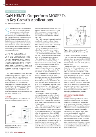
                                               voltage applied to the gate. Unlike d-GaN,   current flow in a GaN device (Image: EPC)
           For a 48-bus system, a              e-GaN devices do not need a negative startup
           250-kHz GaN solution with           bias; with a zero bias on the gate, the device is   cause delay during switching transients.
                                               turned off and does not conduct current.
                                                                                     The reverse-conduction characteristics of a
                                                 The threshold of an e-GaN FET is lower
           double the frequency allows         than that of a silicon MOSFET, yielding a   switching device are important. In a MOSFET,
                                                                                   the voltage drop of a body diode is low and its
           a 35% size reduction, lowers        very low gate-to-drain capacitance (C GD ). The   reverse recovery is very slow, resulting in high
           inductor DCR losses, and cuts       low-capacitance structure permits switch-  switching losses.
                                               ing hundreds of volts in nanoseconds at
                                                                                     GaN devices do not have a reverse body
           system cost by roughly 20%.         megahertz frequencies. GaN FETs’ large gate-  diode; they are able to conduct in the reverse
                                               to-source capacitance (C GS ) relative to C GD    direction because of their physical nature.
                                               gives the devices good dV/dt immunity.   In the case of reverse conduction, it will be
             GaN transistors are significantly faster and   The dV/dt sensitivity of power-switching   necessary to have dead time. A d-GaN device
           smaller than silicon MOSFETs, enabling effi-  devices is caused by the various parasitic   in cascade has reverse recovery by means of
           ciency gains that have opened the door    capacitance and gate-drive circuit impedance   the low-voltage silicon device.
           to applications not possible with silicon    levels. The gate-charge (Q g ) parameter, on   In hard-switching converters, the out-
           technology. Efficient Power Conversion’s   the other hand, indicates the ability of the   put charge is dissipated in the FET at each
           (EPC’s) eGaN FETs are supplied in low-   device to change states quickly, reaching a   power-on transition. This loss is proportional
           inductance, low-resistance, small, and low-  higher dV/dt with minimal switching losses.   to the output charge (Q OSS ), bus voltage, and
           cost land grid array (LGA) and ball grid array   The gate charge of an e-GaN device is 10×   switching frequency. GaN FETs have a signifi-
           (BGA) packages. The new EPC FETs offer   higher than for an equivalent MOSFET, while   cantly lower Q OSS  than silicon FETs, reducing
           designers best-in-class performance com-  d-GaN devices have about a 2× to 5× higher   the output charge loss per cycle and thus
           pared with silicon MOSFETs in both hard- and   Q g  than MOSFETs.       allowing higher frequencies (Figure 2).
           soft-switching applications.          To determine the dV/dt sensitivity of a
                                               power switch, you can use a figure of merit   AUTOMOTIVE AND CONSUMER
           GaN FETs                            called the Miller charge ratio (Q GD /Q GS1 ). A   SOLUTIONS
           GaN switching devices are available in two   Miller charge ratio of <1 will guarantee the   Emerging computing applications demand
           types: enhancement mode (e-GaN) and   theoretical dV/dt immunity. The gate-drive   more power in much smaller form factors.
                                               circuit layout is a critical factor in improving   In addition to the expanding needs of the
                                               dV/dt immunity.                     server market, some of the most challenging
                                                 The d-GaN transistor has the gate structure   applications are multi-user gaming systems,
                                               of a low-voltage silicon MOSFET. Therefore,   autonomous cars, and artificial intelligence.
                                               existing commercial MOSFET gate drivers can   Automotive systems are increasingly
                                               easily operate d-GaN switches. The downside   moving toward 48-V devices, driven by the
                                               is that the addition of the silicon MOSFET   increase in electronically controlled
                                               ignition resistance raises the overall ignition   energy-hungry functions and the emergence
                                               resistance. The increase can be significant   of autonomous vehicles that create additional
                                               for low voltages (<200 V). For higher values   demands on the energy distribution system
                                               (600 V), the additional resistance may be only   from systems such as LiDAR, radar, cameras,
                                               about 5% of total on-resistance. A d-GaN   and ultrasonic sensors. These energy-hungry
                                               transistor also has increased packaging com-  processors represent an additional burden for
           Figure 1: e-GaN (left) and d-GaN    plexity. Parasitic inductance and capacitance   traditional 12-V power distribution buses in
           configurations (Image: EPC)         between the MOSFET and the GaN HEMT may   the automotive sector.

           JUNE 2020 | www.eetimes.eu

