Page 20 - EE Times Europe Magazine | June2020
P. 20
20 EE|Times EUROPE


            WIDE-BANDGAP DEVICES
           SiC MOSFETs for the Next Generation of EVs


           By Maurizio Di Paolo Emilio


             n their efforts to maximize energy efficiency in electric
             and hybrid vehicles, designers are focusing on devices in
             compact packaging and on assembly of high-thermal–
          Ireliability, low-switching–loss power electronics modules.
           Design parameters take into account the power level, con-
           version efficiency, and operating temperature of the vehicle
           powertrain system; thermal energy dissipation capacity; and
           the system package.

           SiC VERSUS GaN
           The bandgap of a semiconductor material refers to the
           energy needed to knock an electron of the material from the
           valence band to the conduction band. Silicon carbide (SiC)
           and gallium nitride (GaN) are wide-bandgap (WBG) semi-
           conductors, meaning this energy level is higher for those
                                        materials than it is for silicon   vice president and general manager of Power at Cree. “Global OEMs
           SiC power electronics        (Si): Si’s bandgap is    have announced more than US$300 billion in EV investments, and we
           for EVs meet the design      1.1 eV, compared with 3.3 eV   expect a projected 20% of all model types manufactured to be electri-
                                                                 fied within the next 10 years.”
                                        for SiC and 3.4 eV for GaN.
                                          Despite the similar
                                                                   GaN performance and reliability are related to temperature and
           requirements for high-       bandgaps of SiC and GaN,   the Joule heating effect on the channel. Substrates such as SiC and
           power applications,          components based on those   diamond integrated into GaN can improve heat management, making it
           thus contributing            materials are not inter-  possible to lower the operating temperature of the device.
                                                                   GaN-on-SiC works very well for very high-frequency (RF) applica-
                                        changeable, and a designer’s
           significantly to system      choice of material will differ   tions and thus is expected to serve future devices that will work with
                                                                 5G. GaN-on-Si, meanwhile, maintains its place in low-voltage (<200-V)
                                        according to the parame-
           performance and long-        ters of use for the systems   products such as compact USB Power Delivery (PD) chargers. In the
           term reliability.            in which the devices will   range between 600 V and 650 V, both technologies work very well in
                                        operate.
                                                                 sub-2-kW applications.
                                          SiC-enriched power elec-  Because of its excellent performance in minimizing switching losses,
           tronics for electric vehicles (EVs) meet the design parameters required   GaN can be the right solution when switching frequencies in the mega-
           in high-power applications and thus contribute significantly to sys-   hertz range are required. But at increased switching frequency and
           tem performance and long-term reliability. “The adoption rate in the    current values, GaN’s weak resistance (2× to 3× greater than SiC’s) can
           electric-vehicle industry has been tremendous,” said Jay Cameron,    limit GaN’s application at high temperatures in terms of both device
                                                                 and system cost.
                                                                   “Due to the massive adoption of silicon carbide in the automotive
                                                                 industry, we see a path for silicon carbide to become the most cost-
                                                                 effective solution in an even wider variety of power supply designs,”
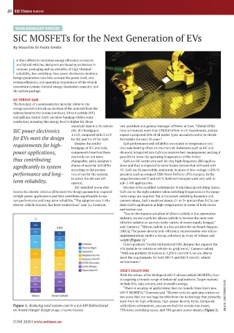
                                                                 said Cameron. “Silicon carbide is a key solution for on-board chargers
                                                                 [OBCs]. The power-density and -efficiency improvements over silicon
                                                                 implementations enable a strong reduction in terms of volume and
                                                                 weight [Figure 1].”
                                                                   Cree’s products “enable bidirectional OBC designs that support the
                                                                 V2x [vehicle-to-vehicle or vehicle-to-grid] trend,” Cameron added.
                                                                 “With our portfolio of devices at 1,200 V and 650 V, we are able to
                                                                 meet the requirements for both 800-V and 400-V electric vehicle
                                                                 architectures.”
                                                                 CREE’S SOLUTIONS
                                                                 With the release of its Wolfspeed 650-V silicon carbide MOSFETs, Cree
                                                                 is targeting a broader range of industrial applications. Target markets
                                                                 include EVs, data centers, and renewable energy.
                                                                   “There is an array of applications that can benefit from Cree’s new
                                                                 650-V MOSFETs,” Cameron said. “Electric vehicles and data centers are
                                                                 two areas that can see huge benefits from the technology that primarily  IMAGE: SHUTTERSTOCK
                                                                 stem from its high-efficiency, high-power-density traits. Compared
           Figure 1: Reducing total system cost in a 6.6-kW bidirectional   with silicon alternatives, you can see half the conduction losses,
           on-board charger design (Image: Cree/Wolfspeed)       75% lower switching losses, and 70% greater power density [Figure 2].

           JUNE 2020 | www.eetimes.eu

