Page 51 - EE Times Europe Magazine | February 2020
P. 51
EE|Times EUROPE   49


              SPECIAL REPORT: INDIA
            Is India Ready for the Next Chip Wave?


            By Faisal Kawoosa


              ndustry, government, and other stakeholders in
              India are cognizant of the electronics industry’s
              potential not only to strengthen the country’s
           Ipresence on the global stage but also to advance
            technology in other domains for the greater
            societal and economic good. Fully exploiting that
            potential, however, has proved elusive.
              New efforts in electronics are unfolding against
            a backdrop of haphazard economic development in
            India. Growth initiatives have been skewed toward
            the country’s urban centers, even as the majority
            of the population remains rural (about 66.46%,
            according to the World Bank), meaning that a large
            percentage of the populace does not see the full
            benefi ts of investment and development. For too many, access to qual-  that are exported out of India and then consumed via products or
            ity infrastructure, education, and health care is a dream unfulfi lled.   components imported into the country. The entire Make in India
              Since 2010, there has been a focus on the role that technology, and   program, including the phased manufacturing-program roadmap for
            especially electronics, can play in harmonizing growth across India. For   components, mainly promotes assembly of electronic systems and
            the chip industry in particular, four pillars of growth have been identi-  components and has done little to foster homegrown manufacturing-
            fi ed  an enabling and visionary policy regime, world-class infrastructure   and engineering-level companies.
            capable of creating world-class products and services, access to adequate   Industry has voiced two primary concerns with respect to imple-
            and easy funding to propel growth, and a deep talent pool with the   mentation of the policy. First, setting up a business under the single
                                proper training to develop intellectual-prop-  policy objective is a time-consuming process that can take years to
                                erty (IP) and knowledge repositories.  implement in a tangible form. Second, the bureaucratic procedures and
                                  The government’s National Policy on   strict guidelines that need to be followed strip risk out of the process
                                Electronics (NPE) 2012 laid out a formal   but leave decision-makers too little leeway for discretionary, creative
                                foundation for growth in the sector. The   problem-solving.
                                recently announced NPE 201  is funda-  While positive overall about the policy,  aswinder Ahuja, corporate
                                mentally aligned with the earlier policy but   vice president and managing director at Cadence Design Systems India,
                                adds initiatives to promote exports out of   said that the country still lags in the implementation and time to
                                India as well as enable the requisite vol-  execute.
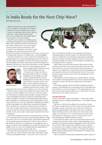
            Faisal Kawoosa      umes to give companies the justifi cation to   P. .G. Menon, president and CEO of  ANN Consulting and former
                                establish operations in the country. Those   president of the India Electronics and Semiconductor Association, took
            goals apply to the entire electronics industry, not just the chip sector.  issue with the one-size-fi ts-all approach. “The implementation of the
              Since the policy framework was created in 2012, government initia-  policy has to be tailor-made  for  the vertical,” Menon said. “We cannot
            tives have included establishment of incubation centers for product   look at each vertical with the same vision.”
            and IP development, modifi ed special incentive packages (M-SIPs) to
            attract investments in the sector, creation of an electronics devel-  THE FAB QUESTION
            opment fund (EDF) to enable more risk-taking and provide funds for   The three weak links in India’s chip industry — semiconductor fabs,
            R&D, establishment of manufacturing clusters, and funding for Ph.D.   incubation centers, and manufacturing clusters — are at different levels
            programs in electronic-systems design and manufacturing. In addition,   of progress.
            a preferential market access (PMA) policy was invoked in February   The house is still divided on whether India should have its own
            2012 to promote the procurement of domestically sourced electron-  fab. Those who argue in favor of a fab presence cite emotional as well
            ics for use in security-related products and by government agencies.   as strategic reasons. Ahuja comes down on the side of a domestic
            Around the same time, the government also approved plans to build   fab but has suggested that 28 nm might be the most economically
            two fabs in India, and a couple of global players expressed their intent   viable technology node for such a facility. Not only would it be less
            to participate.                                       capital-intensive than a 10- or  -nm fab program, but in the history
              Looking at these policy interventions, especially between 2010 and   of semiconductor manufacture, the 2 -nm node has been the lon-
            2014, one would assume that by now, India would have charted a strong   gest-serving and has yielded the highest volumes.
            new growth trajectory for the chip industry. There has been some prog-  As for incubation centers, there are two potentially good ones. Elec-
            ress in manufacturing, especially with the “Make in India” initiative,   tropreneur Park, the fi rst systems-design focused incubation center,
            but overall, the domestic value addition has been negligible, even in   is funded by the Indian government, managed by Software Technology
            marquee products. In mobile handsets, for example, the domestic value   Parks of India (STPI), and located on Delhi University’s south cam-
            addition is not more than 1  , and India still relies signifi cantly on   pus. The other center is Maker’s  illage Cochin, a startup initiative of
            imported components from a global supply chain.       the government Ministry of Electronics and Information Technology
              The small value-add clearly does not result in any real growth in   (MeitY) with the Indian Institute of Technology (IIT) Trivandrum and
            opportunities for the chip industry within India, other than in design   Kerala Startup Mission.
            services and embedded software — contributions to the value chain   These two institutions lead product development and IP creation for

                                                                                       www.eetimes.eu | FEBRUARY 2020

