
Page 10 - PEN eBook May 2023
P. 10
COVER STORY – DESIGN COVER STORY – DESIGN
by up to 64%. Additionally, the maximum temperature The advances in overall device performance are
at the hotspot of the converter on the primary side remarkable, resulting from significant improvements at May 9–11, 2023: Visit us at PCIM Europe in Nuremberg
decreases by 7.5°C. a device technology level. These improvements led to
the creation of a unique device structure, the first to You’re invited to join Infineon’s presentation of the latest
EFFICIENCY MEASUREMENTS UNDER employ a 3D charge compensation in conjunction with trends in silicon power semiconductors and wide-bandgap
SOFT-SWITCHING CONDITIONS: a metal gate in a trench power MOSFET. As a result, technologies at our demo stations, specifically tailored to your
TESTING A 1-KW IBC FOR DATA this technology reduces on-resistance, dramatically application of interest. Discover how our solutions address
CENTERS lowers gate- and gate-drain charges and improves the today’s challenges in green and digital
This 1-kW, 4:1, fixed-frequency LLC IBC operates as a switching homogeneity across the device area. These transformation through our new product
DCX from an input that may vary from 42 V to 60 V. achievements translate into a significant enhancement demos, live TechTalks on stage or
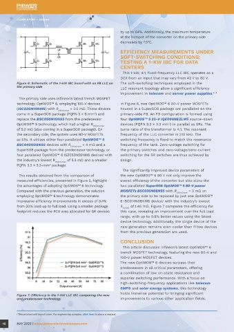
Figure 6: Schematic of the 1-kW IBC board with an FB LLC on The soft-switching techniques employed in the in system efficiency in various applications across personal conversations with our experts.
the primary side LLC resonant topology allow a significant efficiency different load conditions. Meet us at Messe Nürnberg event
improvement in telecom and server power supplies. 6–8 grounds (Hall 7, Booth 412).
The primary side uses Infineon’s latest trench MOSFET The efficiency measurements carried out on several
technology, OptiMOS™ 6, employing 100-V devices In Figure 6, two OptiMOS™ 6 80-V power MOSFETs SMPS applications under both hard- and soft-switching
(ISC030N10NM6) with R DS(on),max = 3.0 mΩ. These devices housed in a SuperSO8 package are paralleled on the conditions confirm the remarkable findings at the
come in a SuperSO8 package (PQFN 5 × 6 mm ) and primary-side FB. An FB configuration is formed using semiconductor device level. Depending on the topology
2
replace the BSC050N10NS5 from the predecessor four OptiMOS™ 5 25-V IQE006NE2LM5 source-down and load condition, it is possible to raise efficiency To learn more about the latest power MOSFET
OptiMOS™ 5 technology, which had a higher R DS(on),max devices (PQFN 3.3 × 3.3 mm ) in parallel as SRs. The by up to 1%, further highlighting the superiority of technology family and its potential to revolutionize the
2
of 5.0 mΩ (also coming in a SuperSO8 package). On turns ratio of the transformer is 4:1. The resonant this new technology. Additionally, the much-improved telecom power arena and other application fields, we
the secondary side, the system uses 80-V MOSFETs frequency of the LLC converter is 310 kHz. The device performance reduces the number of devices encourage you to visit our webpage.
as SRs. It utilizes either four paralleled OptiMOS™ 5 switching frequency is fixed to match the resonance required by up to 50% without any adverse effect on
BSC040N08NS5 devices with R DS(on),max = 4 mΩ and a frequency of the tank. Zero-voltage switching for the device temperature, demonstrating its potential to
SuperSO8 package from the predecessor technology, or the primary switches and zero-voltage/zero-current significantly lower costs and improve overall system
four paralleled OptiMOS™ 6 ISZ053N08NM6 devices with switching for the SR switches are thus achieved by reliability.
i
the industry’s lowest R DS(on),max of 5.3 mΩ and a smaller design.
PQFN 3.3 × 3.3-mm package.
2
The significantly improved device parameters of
The results obtained from the comparison of the new OptiMOS™ 6 80 V not only improve the
measured efficiencies, presented in Figure 5, highlight overall efficiency of the converter but also allow the
the advantages of adopting OptiMOS™ 6 technology. two paralleled SuperSO8 OptiMOS™ 5 80-V power
Compared with the previous generation, the solution MOSFETs BSC030N08NS5 with R DS(on),max = 3 mΩ on
employing OptiMOS™ 6 technology demonstrates the primary side to be replaced by just one OptiMOS™
impressive efficiency improvements in excess of 0.4% 6 ISC014N08NM6 device, with the industry’s lowest
i
from 20% load up to full load. Using a smaller package R DS(on) of 1.45 mΩ. Figure 7 compares the efficiency for
footprint reduces the PCB area allocated for SR devices this case, revealing an improvement over the full load References
range, with up to 0.8% better values using the latest
device technology. Additionally, the single device of the
new generation remains even cooler than if two devices ▶ 1Williams et al. (2017). “The Trench Power MOSFET: Part I - History, Technology, and Prospects.” IEEE
from the previous generation are used. Transactions on Electron Devices, Vol. 64, No. 3, pp. 674–691.
▶ 2Ejury, J., Hirler, F., & Larik, J. (2001). “New P-Channel MOSFET Achieves Conventional N-Channel MOSFET
CONCLUSION Performance.” PCIM.
This article discusses Infineon’s latest OptiMOS™ 6 ▶ 3Schlögl et al. (2005). “A new robust power MOSFET family in the voltage range 80 V – 150 V with superior
trench MOSFET technology, featuring the new 80-V and low RDSon, excellent switching properties and improved body diode.” EPE.
100-V power MOSFET devices.
The new OptiMOS™ 6 devices surpass their ▶ 4Siemieniec et al. (2022). “A new power MOSFET technology achieves a further milestone in efficiency.”
predecessors in all critical parameters, offering EPE.
a combination of low on-state resistance and ▶ 5Li, S. (2020). “Intermediate Bus Converters for High-Efficiency Power Conversion: A Review.” IEEE Texas
superior switching performance. With a focus on Power and Energy Conference (TPEC).
high-switching–frequency applications like telecom
SMPS and solar energy systems, this technology ▶ 6Liu, R., & Lee, C.Q. (1988). “Analysis and design of LLC-type series resonant converter.” IEE Electron
Figure 7: Efficiency in the 1-kW LLC IBC comparing the new holds immense potential for bringing significant Device Letters, Vol. 24, No. 24, pp. 1517–1519.
and predecessor technology improvements to various other application fields. ▶ 7Yang et al. (2002). “LLC resonant converter for front end DC/DC conversion.” APEC.
▶ 8Jung, J., & Kwon, J. (2007). “Theoretical Analysis and Optimal Design of LLC Resonant Converter.” EPE.
i This product will launch soon. For engineering samples, click here to place a request.
10 MAY 2023 | www.powerelectronicsnews.com MAY 2023 | www.powerelectronicsnews.com 11