
Page 8 - PEN eBook May 2023
P. 8
COVER STORY – DESIGN COVER STORY – DESIGN
plate, which was isolated from the gate electrode and low- and medium-voltage power MOSFETs. In order to
instead electrically connected to the source potential also further reduce the FOM = R DS(on) × Q and
g
g
(Figure 1d). While the charge compensation principle FOM = R DS(on) × Q values, the gate trench underwent
gd
gd
operates as before, the buried field plate does not a complete redesign to minimize its lateral extension.
introduce any additional contributions to the However, the substantially smaller dimensions of the
gate-drain capacitance. Instead, the field plate shields gate impose a new challenge, as the use of polysilicon
the gate electrode from the drain potential, which as gate material would result in unacceptably large
reduces the gate-drain capacitance C and related internal gate resistances. The introduction of gate
gd
charges. These devices, at the time of their introduction fingers usually solves this issue, but these reduce the
to the market, showed best-in-class performance with active area available for current conduction.
low gate charge and gate-drain charge characteristics,
high switching speeds and good avalanche ruggedness. 3 Instead, a new metal gate system has been introduced
to avoid any loss of active area, which otherwise would
INFINEON’S INNOVATIVE APPROACH be rather significant. This system not only reduces the
TO RAISING POWER MOSFET DESIGN internal gate resistance but also enhances the gate
TO THE NEXT LEVEL resistance uniformity across the chip. Furthermore,
4
To reach the next level in power MOSFET evolution, the field plates are directly connected to the source
new MOSFET devices are required to provide metal, ensuring a rapid and homogeneous transition at
improvements across all FOMs. This is needed to enable turn-on and turn-off. This minimizes switching losses Figure 3: System diagram of the IBA
high-frequency switched-mode power supply (SMPS) and mitigates the risk of an undesired dv/dt-induced
operation, whereby losses are associated with charges parasitic turn-on of the MOSFET. digital loads (xPUs and ASICs). Depending on the end in these applications, showing typical peak efficiencies
5
(switching) and on-state resistance (conduction). To application, PoL converters can be optimized to operate that exceed 98%, much higher than their regulated
meet these more demanding requirements, a novel BOOSTING END-TO-END CONVERSION either with a narrow or wide input voltage range. counterparts.
cell-design approach has been developed and EFFICIENCY IN TELECOM AND DATA In telecom systems, where the –48-V bus shows wide
implemented, which explores for the first time a true CENTER SYSTEMS tolerance, it has been common for the PoL regulators DEVICE BEHAVIOR AND EFFICIENCY
3D charge compensation. Intermediate bus converters (IBCs) are considered a to operate with a narrow input voltage range (e.g., 12 V), MEASUREMENTS UNDER
demanding application for power MOSFETs. As part of thus requiring a regulated IBC. Taking the burden of the HARD-SWITCHING CONDITIONS:
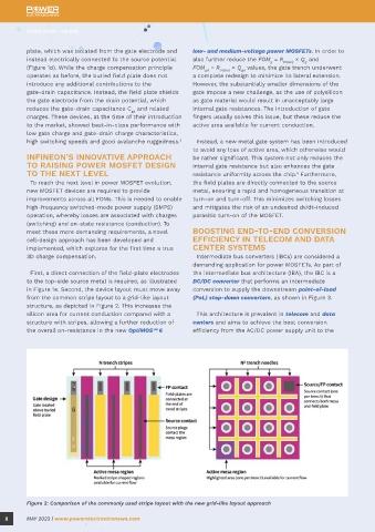
First, a direct connection of the field-plate electrodes the intermediate bus architecture (IBA), the IBC is a regulation from a wide input range TESTING A 600-W IBC FOR TELECOM
to the top-side source metal is required, as illustrated DC/DC converter that performs an intermediate (–36 V to –75 V), the IBC tends to be rather inefficient APPLICATIONS
in Figure 1e. Second, the device layout must move away conversion to supply the downstream point-of-load and plays an important role in defining the The IBC in this application operates as an isolated
from the common stripe layout to a grid-like layout (PoL) step-down converters, as shown in Figure 3. end-to-end conversion efficiency. Improving the IBC DC/DC IBC with a nominal –48-V input (overall range
structure, as depicted in Figure 2. This increases the efficiency is thus paramount to boosting the overall from –36 V to –75 V) and a 12-V output voltage bus.
silicon area for current conduction compared with a This architecture is prevalent in telecom and data conversion efficiency. The fully regulated converter in the industry’s standard
structure with stripes, allowing a further reduction of centers and aims to achieve the best conversion quarter-brick form factor operates at a switching
the overall on-resistance in the new OptiMOS™ 6 efficiency from the AC/DC power supply unit to the In modern data center systems or advanced AI frequency of 250 kHz and can deliver an output current
hardware accelerators, extremely high currents have of a maximum of 50 A. The IBC is based on a
to be supplied to sub-1-V digital loads. The efficiency hard-switching full-bridge (FB) topology with a
of the two stages can be maximized by playing with the center-tapped (CT) synchronous rectifier (SR) on the
down-conversion ratio of the IBC and with the burden secondary side, schematically shown in Figure 4.
of regulation being transferred to the multiphase
PoL/voltage regulator module. Indeed, unregulated IBCs
in the form of DC transformers (DCX) are employed
Figure 4: Simplified schematic of the 600-W IBC board in Figure 5: Efficiency in the 600-W IBC comparing the new and
Figure 2: Comparison of the commonly used stripe layout with the new grid-like layout approach FB-CT configuration predecessor technology
8 MAY 2023 | www.powerelectronicsnews.com MAY 2023 | www.powerelectronicsnews.com 9