
Page 14 - PEN eBook May 2023
P. 14
SEMICONDUCTORS
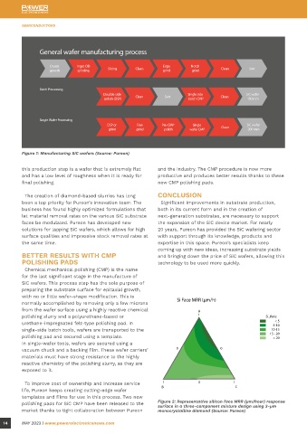
General wafer manufacturing process
Crystal Ingot OD Edge Notch
growth grinding Slicing Clean grind grind Clean Sort
Batch Processing
Double side Single side SiC wafer
polish (DSP) Clean Sort batch CMP Clean 150 mm
Single Wafer Processing
DSP or Fine Pre-CMP Single SiC wafer
grind grind polish wafer CMP Clean 200 mm
Figure 1: Manufacturing SiC wafers (Source: Pureon)
this production step is a wafer that is extremely flat and the industry. The CMP procedure is now more
and has a low level of roughness when it is ready for productive and produces better results thanks to these
final polishing. new CMP polishing pads.
The creation of diamond-based slurries has long CONCLUSION
been a top priority for Pureon’s innovation team. The Significant improvements in substrate production,
business has found highly optimized formulations that both in its current form and in the creation of
let material removal rates on the various SiC substrate next-generation substrates, are necessary to support
faces be modulated. Pureon has developed new the expansion of the SiC device market. For nearly
solutions for lapping SiC wafers, which allows for high 20 years, Pureon has provided the SiC wafering sector
surface qualities and impressive stock removal rates at with support through its knowledge, products and
the same time. expertise in this space. Pureon’s specialists keep
coming up with new ideas, increasing substrate yields
BETTER RESULTS WITH CMP and bringing down the price of SiC wafers, allowing this
POLISHING PADS technology to be used more quickly.
Chemical mechanical polishing (CMP) is the name
for the last significant stage in the manufacture of
SiC wafers. This process step has the sole purpose of
preparing the substrate surface for epitaxial growth,
with no or little wafer-shape modification. This is
normally accomplished by removing only a few microns Si Face MRR (µm/h)
from the wafer surface using a highly reactive chemical A
polishing slurry and a polyurethane-based or 1 Si_Rate
< 5
urethane-impregnated felt-type polishing pad. In 5-10
single-side batch tools, wafers are transported to the 10-15
polishing pad and secured using a template. 15 - 20
> 20
In single-wafer tools, wafers are secured using a
vacuum chuck and a backing film. These wafer carriers’ 0 0
materials must have strong resistance to the highly
reactive chemistry of the polishing slurry, as they are
exposed to it.
To improve cost of ownership and increase service 1 0 1
life, Pureon keeps creating cutting-edge wafer B C
templates and films for use in this process. Two new
polishing pads for SiC CMP have been released to the Figure 2: Representative silicon face MRR (μm/hour) response
surface in a three-component mixture design using 3-μm
market thanks to tight collaboration between Pureon monocrystalline diamond (Source: Pureon)
14 MAY 2023 | www.powerelectronicsnews.com