
Page 7 - PEN eBook May 2023
P. 7
COVER STORY – DESIGN COVER STORY – DESIGN
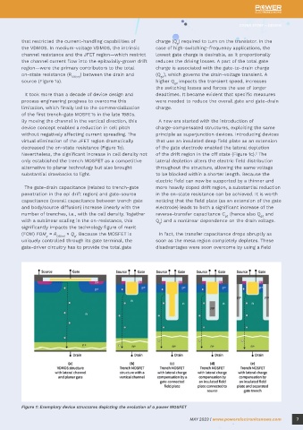
that restricted the current-handling capabilities of charge (Q ) required to turn on the transistor. In the
g
the VDMOS. In medium-voltage VDMOS, the intrinsic case of high-switching–frequency applications, the
channel resistance and the JFET region—which restrict lowest gate charge is desirable, as it proportionally
the channel current flow into the epitaxially-grown drift reduces the driving losses. A part of the total gate
region—were the primary contributors to the total charge is associated with the gate-to-drain charge
on-state resistance (R DS(on) ) between the drain and (Q ), which governs the drain-voltage transient. A
gd
source (Figure 1a). higher Q impacts the transient speed, increases
gd
the switching losses and forces the use of longer
It took more than a decade of device design and deadtimes. It became evident that specific measures
process engineering progress to overcome this were needed to reduce the overall gate and gate-drain
limitation, which finally led to the commercialization charge.
of the first trench-gate MOSFETs in the late 1980s.
By moving the channel in the vertical direction, this A new era started with the introduction of
device concept enabled a reduction in cell pitch charge-compensated structures, exploiting the same
without negatively affecting current spreading. The principle as superjunction devices. Introducing devices
virtual elimination of the JFET region dramatically that use an insulated deep field plate as an extension
decreased the on-state resistance (Figure 1b). of the gate electrode enabled the lateral depletion
Nevertheless, the significant increase in cell density not of the drift region in the off state (Figure 1c). The
2
only established the trench MOSFET as a competitive lateral depletion alters the electric field distribution
alternative to planar technology but also brought throughout the structure, allowing the same voltage
substantial drawbacks to light. to be blocked within a shorter length. Because the
electric field can now be supported by a thinner and
Accelerating the Drive penetration in the epi drift region) and gate-source more heavily doped drift region, a substantial reduction
The gate-drain capacitance (related to trench-gate
in the on-state resistance can be achieved. It is worth
for Higher Efficiencies capacitance (overall capacitance between trench gate noticing that the field plate (as an extension of the gate
electrode) leads to both a significant increase of the
and body/source diffusion) increase linearly with the
reverse-transfer capacitance C (hence also Q and
number of trenches, i.e., with the cell density. Together
gd
gd
Q ) and a nonlinear dependence on the drain voltage.
with a sublinear scaling in the on-resistance, this
Through Power MOSFET significantly impacts the technology figure of merit soon as the mesa region completely depletes. These
g
(FOM) FOM = R
In fact, the transfer capacitance drops abruptly as
× Q . Because the MOSFET is
g
DS(on)
g
uniquely controlled through its gate terminal, the
Technology Innovation gate-driver circuitry has to provide the total gate disadvantages were soon overcome by using a field
Introducing Infineon’s latest OptiMOS™ 6 device
technology—a novel cell-design approach for higher
power densities and cost-effectiveness
By Ralf Siemieniec, Senior Principal Engineer Power Device Development; Simone
Mazzer, Senior Engineer Product Applications; Cesar Braz, Principal Engineer Product
Definition; Michael Hutzler, Lead Principal Engineer Technology Development; David
Laforet, Lead Principal Engineer Technology Development; Ingmar Neumann, Principal
Engineer Technology Development; Elias Pree, Senior Staff Engineer Technology
Development; and Alessandro Ferrara, Principal Engineer Product Concept, all at
Infineon Technologies
MOSFET technology has been widely recognized as switch. Due to its superior switching performance and
1
an excellent option for switches in power management high input impedance, the MOSFET quickly emerged
circuits since its inception. Commercially available as an attractive alternative to bipolar technologies.
since the late 1970s, vertical diffused MOSFET (VDMOS) However, its application in the power electronics
structures were the first to fulfill the need for a power industry was limited by the high on-state resistance Figure 1: Exemplary device structures depicting the evolution of a power MOSFET
6 MAY 2023 | www.powerelectronicsnews.com MAY 2023 | www.powerelectronicsnews.com 7