
Page 15 - PEN eBook July 2022
P. 15
Thermal Management Thermal Management
The PCB has a certain
thickness, influenced by
the number of necessary Cu
layers for circuit design and
a density limitation for the
thermal vias. Because of that,
the effective cross-sectional
area for heat transfer through
the PCB is reduced compared
with the area for heat transfer
offered by the device heatsink.
This is the first bottleneck.
Figure 2: Optimization results of the entire server power supply showing efficiency versus density, with the optimal LLC Figure 4: Example solution using top-side cooling
stage frequency The second bottleneck is the
TIM, having a much lower λ
SMD PACKAGES USED IN SMPS TOPOLOGIES than the device heatsink and the external heatsink.
Infineon offers a larger portfolio of bottom-side cooling (BSC) and top-side cooling (TSC) packages
that fulfill the higher-power and higher-density trends in server switch-mode power supply In some cases, replacing the FR4-based substrate with insulated metal substrate (IMS) allows
(SMPS) applications. This section discusses and compares the different packages concerning for a higher heat flux without exceeding the maximum device or PCB temperature. Especially for
topics such as assembly, thermal performance, and electrical parasitics. single-layer PCB designs, neither thermal vias nor additional TIM are needed. The external heatsink
can be saved because the aluminum core of the board is used as a heatsink. However, although
ASSEMBLY IMPLEMENTATIONS OF BSC AND TSC PACKAGES Z thja is reduced, the number of temperature cycles on board (TCoB) is reduced, especially for
Bottom-side cooling non-leaded SMD packages like TO-leadless (TOLL) or ThinPAK caused by the rigid IMS-based PCB
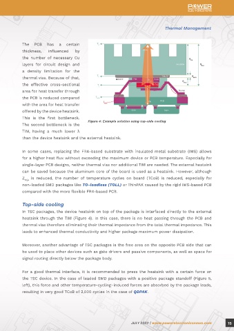
Figures 3 and 4 show the principal cooling concept for BSC and TSC. In both cases, the SMD package is compared with the more flexible FR4-based PCB.
mounted on the PCB, usually via a reflow-soldering process. For BSC, the main heat flux is directed from
the device heatsink (exposed pad) on the bottom of the package through the PCB to an external heatsink Top-side cooling
mounted on the opposite side of the PCB. Therefore, thermal vias below the package and through the In TSC packages, the device heatsink on top of the package is interfaced directly to the external
PCB are needed for heat transfer when using an FR4-based PCB. On the backside of the PCB, the heatsink through the TIM (Figure 4). In this case, there is no heat passing through the PCB and
external heatsink is mounted thermal vias therefore eliminating their thermal impedance from the total thermal impedance. This
on the area with the thermal leads to enhanced thermal conductivity and higher package maximum power dissipation.
vias. The heatsink and the PCB
are electrically separated via Moreover, another advantage of TSC packages is the free area on the opposite PCB side that can
a thermal interface material be used to place other devices such as gate drivers and passive components, as well as space for
(TIM). Quite often, a foil with signal routing directly below the package body.
a thickness in the range of
100–500 μm is used as TIM, For a good thermal interface, it is recommended to press the heatsink with a certain force on
which has, in the best case, the TSC device. In the case of leaded SMD packages with a positive package standoff (Figure 5,
a good thermal admittance left), this force and other temperature-cycling–induced forces are absorbed by the package leads,
(λ). This leads ideally to a low resulting in very good TCoB of 2,000 cycles in the case of QDPAK.
thermal impedance (Z ) for
thja
the overall system.
Figure 3: Example solution using bottom-side cooling
14 JULY 2022 | www.powerelectronicsnews.com JULY 2022 | www.powerelectronicsnews.com 15