
Page 19 - PEN eBook July 2022
P. 19
Thermal Management Thermal Management
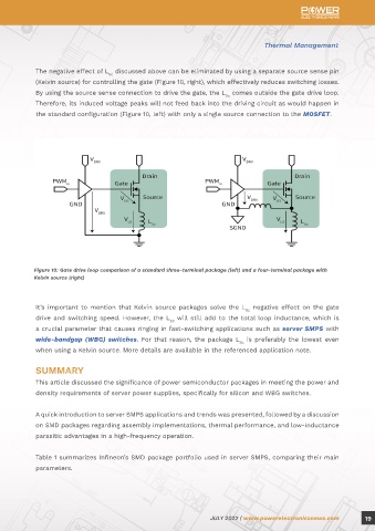
The negative effect of L discussed above can be eliminated by using a separate source sense pin
Sc
(Kelvin source) for controlling the gate (Figure 10, right), which effectively reduces switching losses.
By using the source sense connection to drive the gate, the L comes outside the gate drive loop.
Sc
Therefore, its induced voltage peaks will not feed back into the driving circuit as would happen in
the standard configuration (Figure 10, left) with only a single source connection to the MOSFET.
Figure 9: Example of package source inductance effect on switching on: waveform details (left) and losses (right)
can achieve Z values comparable to THDs. The legend shows that using thin layers of isolation
thja
materials with a comparable high λ is the key to achieving good Z results. Beyond that, using gap
thja
filler and isolation foil with further higher λ will lead to a situation whereby the shown TSC packages
deliver lower Z than the THD.
thja
Low inductance parasitic advantage in high-frequency operation
Figure 10: Gate drive loop comparison of a standard three-terminal package (left) and a four-terminal package with
Figure 9 demonstrates the effect of package source inductance (L ) on the turn-on transient. L is
Sc Sc Kelvin source (right)
increased from 0 to 4 nH. The rise of drain current (di/dt) causes an inductive voltage drop over L ,
Sc
which subtracts from gate drive voltage and thus reduces the gate current. So the voltage transient
takes longer, and the losses increase. The same mechanism but in an opposite manner applies to It’s important to mention that Kelvin source packages solve the L negative effect on the gate
Sc
the turn-off transient. drive and switching speed. However, the L will still add to the total loop inductance, which is
Sc
a crucial parameter that causes ringing in fast-switching applications such as server SMPS with
wide-bandgap (WBG) switches. For that reason, the package L is preferably the lowest even
Sc
when using a Kelvin source. More details are available in the referenced application note.
SUMMARY
This article discussed the significance of power semiconductor packages in meeting the power and
density requirements of server power supplies, specifically for silicon and WBG switches.
A quick introduction to server SMPS applications and trends was presented, followed by a discussion
on SMD packages regarding assembly implementations, thermal performance, and low-inductance
parasitic advantages in a high-frequency operation.
Table 1 summarizes Infineon’s SMD package portfolio used in server SMPS, comparing their main
parameters.
Table 1: Overview of THD and SMD BSC and TSC packages for server applications. For assessment of package
inductance, a device with a similar R inside the package is assumed
DS(on)
18 JULY 2022 | www.powerelectronicsnews.com JULY 2022 | www.powerelectronicsnews.com 19