
Page 17 - PEN eBook December 2022
P. 17
SEMICONDUCTORS Semiconductors
The cascode configuration
makes the part convenient to
use with easy gate drive but
diminishes controllability. The
cascode switching speed is
largely defined by the JFET
gate-drain capacitance and
the internal series resistor
R from JFET gate to the
G
Si-MOSFET source. R is
G
a predefined value and is
inaccessible. The Si-MOSFET
gate has limited effect on
speed because there is
virtually no JFET drain-source
capacitance which would
otherwise feed current back to
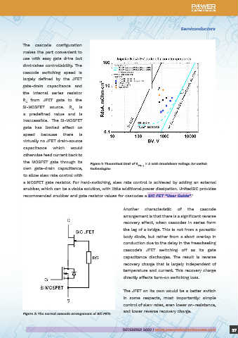
Approaching the the MOSFET gate through its Figure 1: Theoretical limit of R DS(on) × A with breakdown voltage for switch
own gate-drain capacitance,
technologies
Perfect Switch with to allow slew rate control with
a MOSFET gate resistor. For hard-switching, slew rate control is achieved by adding an external
snubber, which can be a viable solution, with little additional power dissipation. UnitedSiC provides
SiC JFETs recommended snubber and gate resistor values for cascodes a SiC FET “User Guide”. 2
Another characteristic of the cascode
By Jonathan Dodge, senior applications engineer at UnitedSiC/Qorvo
arrangement is that there is a significant reverse
recovery effect, when cascodes in series form
SiC JFETs are robust, with high-energy avalanche and short-circuit withstand ratings, and significantly, the leg of a bridge. This is not from a parasitic
they beat all other technologies for the FOM on-resistance per unit die area R × A, achieving a body diode, but rather from a short overlap in
DS(on)
value close to the theoretical limit for the material (Figure 1). This figure of merit directly relates to conduction due to the delay in the freewheeling
the practical performance of the switch and its economy, with more die per wafer for comparable cascode’s JFET switching off as its gate
performance than competing technologies. capacitance discharges. The result is reverse
recovery charge that is largely independent of
CAN WE DO BETTER STILL? temperature and current. This recovery charge
SiC cascodes from UnitedSiC (now Qorvo) have a significant edge in many applications, but can they directly affects turn-on switching loss.
1
be better? The device comprises a SiC JFET and Si-MOSFET in a cascode arrangement to achieve
a normally-off characteristic. Looking at the detail, a cascode is formed as in Figure 2 with the The JFET on its own would be a better switch
Si-MOSFET switching the source of the SiC JFET so that when the Si-MOSFET is off, the JFET source in some respects, most importantly: simple
floats positive, turning the JFET off. When the MOSFET is on, the JFET gate and source are effectively control of slew rates, even lower on-resistance,
shorted, turning it on. and lower reverse recovery charge.
Figure 2: The normal cascode arrangement of SiC FETs
26 DECEMBER 2022 | www.powerelectronicsnews.com DECEMBER 2022 | www.powerelectronicsnews.com 27