Page 21 - PEN eBook December 2022
P. 21
SEMICONDUCTORS                                                                            Semiconductors


            To maximize the potential of a novel semiconductor technology, the industry must make a concerted
            effort to solve technical obstacles that hinder performance. Significant technological advancement
            has taken place in the field of ultra-wide–bandgap semiconductors since 2016, when Flosfia, a

            spinoff from Kyoto University specialized in R&D and commercialization of gallium oxide thin films,
            concluded that gallium oxide warranted development.


            The semiconductor industry is increasingly moving  toward implementing devices built  from
            wide-bandgap materials such as silicon carbide and gallium nitride, but the cost of those materials
            remains relatively high. In response, researchers more recently have pursued development of
            beta-gallium oxide (β-Ga O ), a stable phase of  the compound.  β-Ga O  development is a
                                      2  3                                            2  3
            result of an increased  focus on materials research  to improve  the overall performance of
            power-electronic devices over the junction-based approaches of the past. β-Ga O  stands out for its
                                                                                         2  3
            intrinsic properties, including an ultra-high bandgap (an energy gap of 5 eV), good conductivity and
            field-holding capacity, and high critical field strength, with the highest ever demonstrated being
            5.5 MV/m.


            Processing the material in different ways can result in a variety of properties, demonstrating its
            flexibility. For example, doping the material from a melt results in a resistivity of 10 mΩ-cm; silicon
            implantation can decrease it to 1 mΩ-cm. Halide vapor epitaxy on the material can be controlled to

            have a doping concentration in the range of 10  to 10  cm .
                                                                19
                                                                     –3
                                                          15
            Fabricating      standard
            features onto  β-Ga O
 Gallium Oxide: A   is also relatively easy.
                                     3
                                   2
            For  example,  ohmic  and
 Next-Gen   Schottky contacts can
            be made using standard

 Semiconductor for   metals  like  titanium,
            aluminum,  and  nickel  at
            relatively low annealing
 Power Devices  temperatures.


            Wafering and lapping of
 By Maurizio Di Paolo Emilio  the material can be done

            using standard production

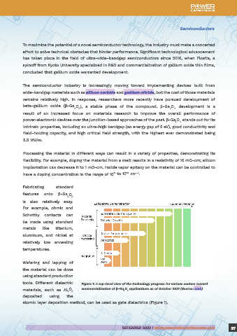
 In the past decade, gallium oxide has seen fast technical development, propelling it to the forefront   tools.  Different  dielectric   Figure 1: A top-level view of the technology progress for various sectors toward
 of ultra-wide–bandgap semiconductor technologies. The major targeted application space is power   materials,  such  as  Al O    commercialization of β-Ga O  applications as of October 2021 (Source: Link)
                                                               2
                                                                 3
                                   2  3
 electronics,  in which  gallium  oxide’s  intrinsic  material  properties  —  high  critical field  strength,   deposited  using  the
 widely tunable conductivity, low mobility, and melt-based bulk growth — promise to deliver the   atomic layer deposition method, can be used as gate dielectrics (Figure 1).
 required high performance at low cost.


 36  DECEMBER 2022 | www.powerelectronicsnews.com             DECEMBER 2022 | www.powerelectronicsnews.com           37

