Page 40 - PEN Ebook May 2021
P. 40
Semiconductors                                                                                                                                                                                             Semiconductors


                                                                                                                                                                                                       combined with a current probe

                                                                                                                                                                                                       TCP312A (30 A, 100 MHz) [14].

                                                                                                                                                                                                       Results and Analysis

                                                                                                                                                                                                       The conditions that have been
                                                                                                                                                                                                       used for this experiment were
                                                                                                                                 Table 1: features of FSM during Turn on state.                        vdc= 600 /400 V, iL=15 A, and
                                                                                                                                                                                                       Rg (ex) varies from 10 to 47
                                                                                                                                                                                                       Ω [14]. Calculation of the vds
                                                                                                                                                                                                       involves the voltage drops on

                                                                                                                                                                                                       them as the practical measure-
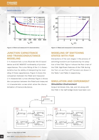
          Figure 2: fitted and measured CV characteristics.    Figure 3: fitted and measured IV characteristics.                                                                                       ment in the lead inductances
                                                                                                                                                                                                       of the MOSFET (Ld and Ls).
          JUNCTION CAPACITANCE                                 MODELING OF SWITCHING                                                                                                                   From the simulation results
          AND TRANSCONDUCTANCE                                 STATES WITH FSM                                                   Table 2: features of FSM during Turn off state.                       it can be clearly stated that

          MODELING                                             Interactions of the sub-stages in the process of                  nected with the source that provides the voltage/    the analytical model can be used to assess the
          C-V characteristic curves illustrate the Si based    switching transient are illustrated by the adop-                  current that is necessary for achieving the con-     switching characteristics of the SiC MOSFET. The

          device and SiC MOSFET nonlinearity of junction       tion of the FSM. Figure 4 shows the flow chart of                 version between the signal interfaces and elec-      results have also shown that the high frequency
          capacitances. The curve fitting of the C-V charac-   the FSM. Significant features of the FSM during                   trical interfaces [14]. Table 3 shows the values of   EMI can be reduced but at the cost of switching
          teristics has the ability of interpreting the mod-   the Turn-on and Turn-off Transient are shown in                   the parasitic parameters.                            loss [14].
          eling of these capacitances. Figure 2 shows the      the Table 1 and Table 2 respectively.
          comparison between the fitted and measured                                                                             Experiment Setup
          C-V characteristic curves whereas Figure 3 shows                                                                       Fig.5 shows the setup of the experiment. In this     CONCLUSION
          the comparison between the fitted and measured       SIMULATION AND EXPERIMENT                                         experiment C3M0120090D and CVFD20065A                Analytical modeling that is based on the FSM has
          I-V characteristic curves which allow the charac-    Simulation Environment                                            from Wolfspeed are chosen as the SiC MOSFET          been elaborated for the evaluation of the switch-
          terization of transconductance.                      Output terminals (Vds, Vak, and Id) along with                    and SiC SBD [14]. A double pulse signal has been     ing characteristics in terms of transient response

                                                               the FSM in the half-bridge block have been con-                   used to govern the gate drive that is generated      speed, switching loss and HF EMI noise for SiC
                                                                                                                                 from the DSPc [14]. Lecroy Wave-Runner 8404-M        MOSFET has been explained in this article. FSM
                                                                                                                                 is used for obtaining the switching waveforms.       is used to model the switching transient analyt-
                                                                                                                                 Voltage probe PPE2KV (2 kV, 400 MHz) is used to      ically, it is responsible for the characterization
                                                                                                                                 measure the voltage of the drain source whereas      and analysis of each sub-stage in the transition
                                                                                                                                 the drain current is measured with the help of
                                                                                                                                 the scaled-down current transformer (CT) that is


          Figure 4: Flow Chart of FSM.                                                                                           Table 3: value of parasitic parameters.              Figure 5: Experimental Setup.

  40      MAY 2021 | www.powerelectronicsnews.com                                                                                                                                              MAY 2021 | www.powerelectronicsnews.com      41

