Page 10 - PEN Ebook May 2021
P. 10
Cover Story - Design Cover Story - Design
Figures 5 and 6 show the effi-
ciency of the presented demo
board. The measured efficiency
includes the bias consumption
but not the power consumption
of the fan. Regarding the input
current performance, the pow-
er factor is over 0.95 when the
load is higher than 20 percent of
the nominal output power and
a THD under 5 percent for an
output power over 50 percent of
Figure 4: Prototype of the 3.3 kW totem-pole PFC board implemented with
CoolMOS™ CFD7 and S7 SJ MOSFETs. the nominal one. The maximum
efficiency is over 98.9 percent in
after t . For this case, the pulse applied to the the range of 1000 W to 1500 W output power and
6
pre-charge MOSFET Q3 becomes effective and over 98 percent for the measured power range.
causes the charge of Q1 C OSS to the depletion With the CoolMOS™ CCM totem-pole PFC solution,
voltage by the C HS_DP –Q3-D1-Q1 network. Once the next level of silicon-based efficiency can be
Q2 is turned on, its drain-to-source voltage will reached, making it a cost-attractive alternative that
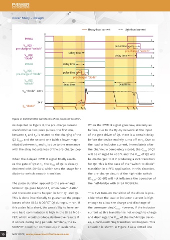
Figure 3: Commutation waveforms of the proposed solution. drop again close to zero, and a smooth transition complements our powerful offering of wide-band-
As depicted in Figure 3, the pre-charge current When the PWM B signal goes low, similarly as “switch to diode” is achieved without severe hard gap solutions.
waveform has two peak pulses, the first one, before, due to the Ry-Cy network at the input switching.
between t and t , is related to the charging of the of the gate driver of Q1, there is a certain delay
3
2
Q2 C OSS , and the second one (with a lower mag- before the device entirely turns off at t . Due to
5
nitude) between t and t is due to the resonance the load or inductor current, immediately after EXPERIMENTAL
4
3
with the stray inductances of the pre-charge loop. the channel is completely closed, the C OSS of Q1 RESULTS ON
will be charged to 400 V, and the C OSS of Q2 will INFINEON’S DEMO
When the delayed PWM B signal finally reach- be discharged to 0 V producing a ZVS transition BOARD
es the gate of Q1 at t , the C OSS of Q2 is already for Q2. This is the case of the “switch to diode” The concept presented in this
4
depleted with 20~24 V, which sets the stage for a transition in a PFC application. In this situation, article has been tested in a
diode-to-switch smooth transition. the pre-charge circuit of the high-side switch 3.3 kW totem-pole bridgeless
Table 1: Infineon products used in the 3.3 kW totem-pole evaluation board with Si
(C HS_DP -Q3-D1) will not influence the operation of PFC, switching at 65 kHz and SJ CoolMOS™
The pulse duration applied to the pre-charge the half-bridge with Si SJ MOSFETs. using SMD components.
MOSFET Q4 goes beyond t when commutation CONCLUSION
4
and transient events happen in both Q1 and Q2. This ZVS turn-on transition of the diode is pos- The demo board shown in Figure 4 is a system Using a simple and effective pre-charge circuit,
This is done intentionally to guarantee the proper sible when the load or inductor current is high solution from Infineon Technologies and imple- which allows the depletion of the Si SJ MOSFETs
losses of the Si SJ MOSFET Q1 during turn-on. If enough to allow the charge and discharge of ments the power switches, diodes, drivers, and and thus brings Q OSS and Q losses to a minimum,
rr
this pulse falls short, the possibility to have se- the corresponding C OSS . However, if the inductor controller presented in Table 1. The pre-charge Infineon now enables the usage of Si SJ MOS-
vere hard commutation is high in the Si SJ MOS- current at this transition is not enough to charge circuit has been designed according to [5], and FETs in CCM totem-pole PFC applications.
FET, which would produce destructive results if and discharge the C OSS of the half-bridge devic- it is implemented according to the design values
it occurs during long periods. Similarly, the LV es, a hard-switching transition will happen. This compiled in Table 2. This article demonstrated the working principles
MOSFET could run continuously in avalanche. situation is shown in Figure 3 as a dotted line of this innovative concept and the experimental
10 MAY 2021 | www.powerelectronicsnews.com MAY 2021 | www.powerelectronicsnews.com 11

