
Page 21 - PEN_Ebook_December_2021
P. 21
Semiconductors DESIGN
GaN CHALLENGES
Historically, the main challenges to overcome to achieve an ever-increasing diffusion of GaN
technology have been reliability and price. The first issues relating to reliability have been largely
resolved, with commercial devices capable of guaranteeing a mean time to failure of over 1 million
hours by operating at a junction temperature above 200˚C. Although early GaN devices were
much more expensive than competing technologies such as silicon, the price gap has narrowed 3D Multi-PCB Design
significantly from initial GaN production on 2- to 4-inch wafers to 6-inch wafers and, lately, 8-inch
(200-mm) wafers. Recent developments and ongoing process improvements will continue to reduce Achieves Greater
the manufacturing cost of GaN devices, making its price even more competitive.
Density in FSBB
Converters
By Stefano Lovati, technical writer for EEWeb
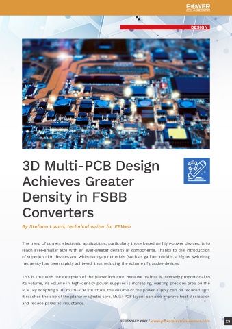
The trend of current electronic applications, particularly those based on high-power devices, is to
reach ever-smaller size with an ever-greater density of components. Thanks to the introduction
of superjunction devices and wide-bandgap materials (such as gallium nitride), a higher switching
For More Information frequency has been rapidly achieved, thus reducing the volume of passive devices.
This is true with the exception of the planar inductor. Because its loss is inversely proportional to
▶ 10 Things to Know about GaN its volume, its volume in high-density power supplies is increasing, wasting precious area on the
PCB. By adopting a 3D multi-PCB structure, the volume of the power supply can be reduced until
▶ The Next Wave of Gallium Nitride it reaches the size of the planar magnetic core. Multi-PCB layout can also improve heat dissipation
and reduce parasitic inductance.
24 DECEMBER 2021 | www.powerelectronicsnews.com DECEMBER 2021 | www.powerelectronicsnews.com 25