
Page 43 - PEN eBook October 2025
P. 43
DESIGN DESIGN
EMS CONSIDERATIONS AND PCB boards are of CTI Class III, slots should be
RECOMMENDED SOLUTIONS made to ensure adequate creepage.
FOR INSULATION MONITORING
APPLICATIONS ▶ Special attention should be paid to PCB traces
In new energy vehicles, the reliability of electronic to ensure sufficient common-mode interference
components is critical to overall vehicle performance. rejection. Considering the effects of distributed
Particularly in environments with harsh EMI, ensuring parasitic capacitance, placing traces too close
that integrated units operate normally and meet within the same layer or across layers should be
electromagnetic compatibility (EMC) standards becomes avoided to prevent the generation of parasitic
a key challenge. Figure 5: Equivalent model for system ESD test low-impedance paths that allow interference
currents to directly enter the chip’s
Some EMS tests, such as radiated immunity, bulk To prevent the aforesaid EMC issues from affecting high-voltage side D and D pins. Additionally,
2
1
current injection (BCI), and portable transmitter immunity, or damaging the chip, the following recommended Figure 6: Suboptimal insulation monitoring design large ground planes near ferrite beads should be
can be equivalently modeled as applying a high-frequency schematic and layout designs are provided. avoided to prevent currents from bypassing the
current source across the high- and low-voltage sides
of the chip, as shown in Figure 4. Despite parasitic Recommended application circuit analysis
capacitances on the PCB and in space providing paths As shown in Figure 1, in insulation monitoring
for high-frequency current discharge, some currents applications, it is recommended to place SSRs at both
may still be directly injected into the chip. At higher sides of the midpoint of the bridge and connect them
frequencies (e.g., several hundred megahertz), isolation to the high-voltage bus V BUS+ and V BUS− via large voltage
capacitors exhibit relatively low impedance, creating divider resistors R and R . Taking K as an example, due
1
2
1
potential current paths. When no other high-frequency to the presence of large voltage divider resistors on the
current discharge paths are designed, these currents may lines between the D and D pins of K and the high-
1
2
1
flow through the isolation capacitors and flow from the voltage bus HV and HV , high-frequency interference
+
−
high-voltage side back to the low-voltage side, forming currents find it difficult to enter the SSR. Additionally,
a current loop that could interfere with normal chip when K is turned on, it provides an additional path
3
operation. for high-frequency interference currents to discharge.
During interference injection, the current flow path
would be: V BUS+ → R → K ’s R DS(on) → K ’s R DS(on) → chassis
1
3
1
ground GND, avoiding flow through the SSR isolation
capacitor and thus reducing the SSR’s malfunction risk
due to interference. It is also recommended to add
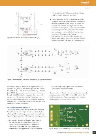
ferrite beads in series with the low-voltage side of the Figure 7: Recommended schematic diagram for insulation monitoring
chip to increase the impedance of the line, thereby
hindering high-frequency currents from entering
the chip. Considering that isolation capacitors have ground GND. Instead, they flow through the isolation beads through stray capacitance, which would
lower impedance at higher frequencies, ferrite beads capacitor of K back to the chassis ground. The current compromise their effectiveness.
2
with higher impedance in the 100- to 400-MHz range flow path is: H → K ’s isolation capacitor C → chassis
ISO
2
V−
Figure 4: Equivalent model for some EMS tests are recommended to effectively block interference ground GND. Because the interference current flows Experimental verification shows that the recommended
currents. During system ESD testing in power-off through the SSR’s isolation capacitor, there is an SSR circuit passes the ISO11452-4 Level 4 BCI test in the
During the design validation phase of BMS products, mode, ESD voltages are applied between V BUS+ , V BUS− , malfunction risk. Moreover, during the system ESD 100-kHz to 400-MHz frequency range and meets the
system-level electrostatic discharge (ESD) tests and the chassis ground GND. For K , K , and K , the test, the ESD voltage is directly borne by the isolation ±10-kV system ESD test requirements.
2
3
1
are required, including power-off mode test, which megaohm-level current-limiting resistors in the ESD capacitor of K , potentially leading to chip damage if the
2
simulate ESD events caused by human contact during path protect the chip. applied ESD voltage is too high.
manufacturing, assembly, testing, storage, and handling
to evaluate the product’s resistance to ESD damage. In In the suboptimal circuit design illustrated in Recommended PCB layout
this test, the ESD gun’s ground must be connected to Figure 5, unlike the design in Figure 1, K and R positions PCB layout is crucial for EMS performance. Based on
2
2
the equipment enclosure ground, and discharge points are swapped, directly connecting K to HV . This results the optimized circuit design discussed previously, the
2
−
include exposed components (e.g., enclosure, screws) in different EMS and ESD performances for K and K . following PCB circuit design reference is provided. See
2
1
and every pin of accessible connectors. Typically, a ±8-kV Without the blocking effect of large voltage divider Figure 7, Figure 8, and the following PCB layout guidelines:
test is required. Because SSRs bridge the high-voltage resistors, high-frequency currents directly inject into K
2
and low-voltage domains of the BMS, improper chip via the D pin. Due to the presence of large voltage divider ▶ To meet the isolation and safety requirements,
2
placement may expose the isolation barrier to the ±8-kV resistor R between the D pin of K and the midpoint the primary and secondary sides must be
2
1
2
ESD voltage without alternative ESD current discharge of the bridge, the impedance of the isolation capacitor physically isolated. Creepage distances and
paths. The equivalent model of the test is shown in becomes relatively smaller, preventing interference clearances must meet the applicable safety
Figure 5. currents from discharging through K to the chassis standards for the application. Given that typical Figure 8: Recommended PCB layout for insulation monitoring
3
42 OCTOBER 2025 | www.powerelectronicsnews.com OCTOBER 2025 | www.powerelectronicsnews.com 43