
Page 47 - PEN eBook October 2025
P. 47
SEMICONDUCTORS SEMICONDUCTORS
This process uses silicon sludge, which could be
waste generated, for example, during the slicing
process of the manufacture of silicon substrates.
Carbon dioxide (CO ) is the other input used in
2
this process. CO is a greenhouse gas, and its
2
capture and reuse in the production of a valuable
raw material essential for SiC wafer manufacturing
showcases a technique that can lower the overall
environmental impact in SiC device manufacturing. In
Tohoku University’s process, microwaves were used
to heat the silicon sludge and create the reaction
with CO through the process of mineralization.
2
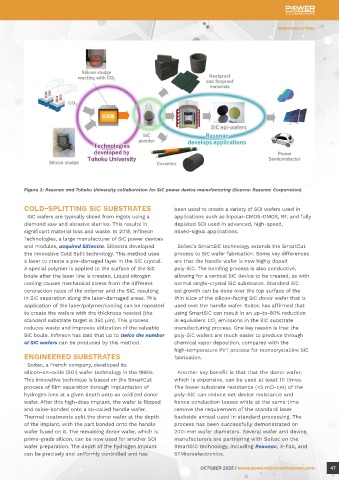
Figure 2 showcases this innovative waste-reusage
technology for the application of SiC power device
manufacturing.
Figure 1: Depiction of the Acheson process and the
alternative Tohoku University process for manufacturing In July 2025, Resonac and Tohoku University
SiC powder announced that basic research into this process has
been completed. This includes the characterization
front-end manufacturing chemicals such as gases, of the SiC crystals obtained through the use Figure 2: Resonac and Tohoku University collaboration for SiC power device manufacturing (Source: Resonac Corporation)
solvents, and slurries, back-end materials such as of SiC powder using this new mineralization
encapsulants and molds, epitaxial wafers, LED chips, method. Comprehensive studies for the practical
and more. SiC epitaxial wafers are part of its product implementation of this are now being pursued. It COLD-SPLITTING SiC SUBSTRATES been used to create a variety of SOI wafers used in
portfolio. Tohoku University conducted research aimed is estimated that 100 tons of SiC powder produced SiC wafers are typically sliced from ingots using a applications such as bipolar-CMOS-DMOS, RF, and fully
at creating an environmentally friendly manufacturing would lead to the equivalent reduction of 110 tons diamond saw and abrasive slurries. This results in depleted SOI used in advanced, high-speed,
process for SiC powder, which is a key starting point of CO . It also allows the recycling of silicon sludge significant material loss and waste. In 2018, Infineon mixed-signal applications.
2
for SiC wafer manufacturing. Figure 1 depicts the waste produced in the large-scale manufacturing of Technologies, a large manufacturer of SiC power devices
comparison between the traditional Acheson process CMOS devices. and modules, acquired Siltectra. Siltectra developed Soitec’s SmartSiC technology extends the SmartCut
and the method developed by Tohoku University. the innovative Cold Split technology. This method uses process to SiC wafer fabrication. Some key differences
a laser to create a pre-damaged layer in the SiC crystal. are that the handle wafer is now highly doped
A special polymer is applied to the surface of the SiC poly-SiC. The bonding process is also conductive,
boule after the laser line is created. Liquid nitrogen allowing for a vertical SiC device to be created, as with
cooling causes mechanical stress from the different normal single-crystal SiC substrates. Standard SiC
contraction rates of the polymer and the SiC, resulting epi growth can be done over the top surface of the
in SiC separation along the laser-damaged areas. This thin slice of the silicon-facing SiC donor wafer that is
application of the laser/polymer/cooling can be repeated used over the handle wafer. Soitec has affirmed that
to create the wafers with the thickness needed (the using SmartSiC can result in an up-to-80% reduction
standard substrate target is 350 µm). This process in equivalent CO emissions in the SiC substrate
2
reduces waste and improves utilization of the valuable manufacturing process. One key reason is that the
SiC boule. Infineon has said that up to twice the number poly-SiC wafers are much easier to produce through
of SiC wafers can be produced by this method. chemical vapor deposition, compared with the
high-temperature PVT process for monocrystalline SiC
ENGINEERED SUBSTRATES fabrication.
Soitec, a French company, developed its
silicon-on-oxide (SOI) wafer technology in the 1990s. Another key benefit is that that the donor wafer,
This innovative technique is based on the SmartCut which is expensive, can be used at least 10 times.
process of film separation through implantation of The lower substrate resistance (<5 mΩ-cm) of the
hydrogen ions at a given depth onto an oxidized donor poly-SiC can reduce net device resistance and
wafer. After this high-dose implant, the wafer is flipped hence conduction losses while at the same time
and oxide-bonded onto a so-called handle wafer. remove the requirement of the standard laser
Thermal treatments split the donor wafer at the depth backside anneal used in standard processing. The
of the implant, with the part bonded onto the handle process has been successfully demonstrated on
wafer fused on it. The remaining donor wafer, which is 200-mm wafer diameters. Several wafer and device
prime-grade silicon, can be now used for another SOI manufacturers are partnering with Soitec on the
wafer preparation. The depth of the hydrogen implant SmartSiC technology, including Resonac, X-Fab, and
can be precisely and uniformly controlled and has STMicroelectronics.
46 OCTOBER 2025 | www.powerelectronicsnews.com OCTOBER 2025 | www.powerelectronicsnews.com 47