Page 40 - PEN eBook October 2025
P. 40

DESIGN                                                                                                                                                                                                                 DESIGN

                                                              considerations:                                                                                                         The luminous intensity of LEDs will degrade over
                                                                                                                                           R , R 2                  1 MΩ             time. According to service life predictions by major
                                                                                                                                            1
                                                               ▶  ADC input voltage consideration: The voltage                                                                       optocoupler suppliers, after 1,000 hours of operation,
                                                                 across R  must always remain below the                                    R , R 4                  6 MΩ             the threshold current will increase by 10%; after
                                                                                                                                            3
                                                                        5
                                                                 maximum input voltage of the ADC, ideally close                                                                     11 years, the threshold current may rise by a factor
                                                                 to its full-scale range to ensure high output                               R 5                   12 kΩ             of over 5. If the design strictly follows the threshold
                                                                 accuracy of the ADC. Therefore,                                                                                     current specified in the datasheet, insufficient optical
                                                                 R  ÷ (R  + R ) × V BUS  should be near the ADC’s                Table 2: Recommended resistor values for 800-V systems  energy received by the photodiode will lead to
                                                                       4
                                                                           5
                                                                  5
                                                                 maximum input voltage, determining the ratio                                                                        bit-error failures. The only solution is to increase the
                                                                 between R  and R .                                              Relay selection                                     input current to compensate for LED aging. However,
                                                                                4
                                                                          5
                                                                                                                                  When the insulation resistance degrades below      this introduces another challenge: Higher current
                                                               ▶  ADC internal impedance consideration: Because                  500 × V BUS , the system must detect this condition and   means elevated temperatures, which degrade both
                                                                 R  serves as the ADC sampling input, its                        trigger an alarm. Taking a system with              the LED’s electro-optical conversion efficiency and
                                                                  5
                                                                 resistance should be significantly lower than the               V BUS  = 800 V as an example, the insulation resistance   the photodiode’s optical-to-electrical conversion
                                                                 internal impedance of the ADC                                   must be greater than 400 kΩ per industry standards. If   performance. Additionally, due to thermal stress and
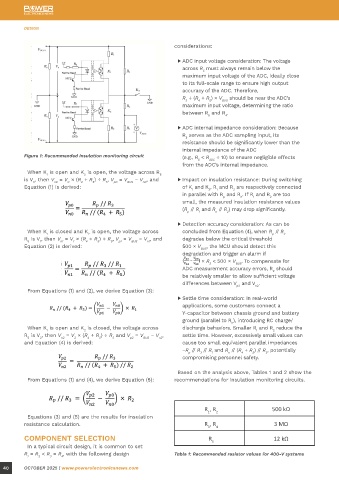
          Figure 1: Recommended insulation monitoring circuit    (e.g., R  < R ADC  ÷ 10) to ensure negligible effects           the leakage current through K  and K  is less than 1 μA,   aging, PhotoMOS devices are typically limited to a
                                                                                                                                                                 2
                                                                                                                                                           1
                                                                       5
                                                                 from the ADC’s internal impedance.                              their equivalent impedance exceeds 800 MΩ, far higher   maximum operating temperature of 85°C. These factors
           When K  is open and K  is open, the voltage across R                                                                  than the insulation resistances R  and R , introducing   pose significant reliability challenges for optocoupler
                               2
                                                                                                                                                                    n
                 1
                                                         5
                                                                                                                                                              p
          is V , then V  = V  × (R  + R ) ÷ R , V  = V BUS  − V , and   ▶  Impact on insulation resistance: During switching     a measurement error of less than 0.05%. If the leakage   products.
                                         p0
                                      5
                                                   n0
                                  5
                             4
                         0
             0
                    n0
          Equation (1) is derived:                               of K  and K , R  and R  are respectively connected              current increases to 10 μA, the equivalent impedance
                                                                             1
                                                                    1
                                                                                   2
                                                                          2
                                                                 in parallel with R  and R . If R  and R  are too                drops to 400 MΩ, causing a measurement error of      Replacing PhotoMOS relays (similar to optocouplers)
                                                                                                2
                                                                                          1
                                                                                     n
                                                                               p
                                                                 small, the measured insulation resistance values                approximately 0.5%.                                 with SSRs that adopt capacitive or magnetic isolation
                                                                 (R  // R  and R  // R ) may drop significantly.                                                                     mechanism can significantly improve system reliability.
                                                                       1
                                                                                 2
                                                                             n
                                                                   p
                                                                                                                                  Therefore, higher leakage currents introduce larger   The NSI7258 from Novosense is a high-reliability
                                                               ▶  Detection accuracy consideration: As can be                    measurement errors. Using Novosense SSR products    isolation device that meets the electromagnetic
           When K  is closed and K  is open, the voltage across   concluded from Equation (4), when R  // R                      with small leakage current (<1 μA) to enable turn-on   interference (EMI) CISPR25 Class 5 standard.
                                2
                                                                                                     3
                 1
                                                                                                 p
          R  is V , then V  = V  × (R  + R ) ÷ R , V  = V BUS  − V , and   degrades below the critical threshold                 and turn-off functions of K  and K  will help enhance   Combining robust technological innovation with
               1
                           1
                               4
           5
                      n1
                                   5
                                           p1
                                        5
                                                     n1
                                                                                                                                                               2
                                                                                                                                                        1
          Equation (2) is derived:                               500 × V BUS , the MCU should detect this                        measurement accuracy and avoid false alarms.        automotive quality management systems, the NSI7258
                                                                 degradation and trigger an alarm if                                                                                 offers a high-performance, high-reliability solution for
                                                                        × R  < 500 × V BUS . To compensate for                   Impact of relay reliability on system safety        insulation monitoring systems.
                                                                           2
                                                                 ADC measurement accuracy errors, R  should                       Traditional mechanical relays suffer from limited
                                                                                                 2
                                                                 be relatively smaller to allow sufficient voltage               switching cycles. Once the maximum number of
                                                                 differences between V  and V .                                  switching cycles is reached, the insulation monitoring
                                                                                           n2
                                                                                    p2
           From Equations (1) and (2), we derive Equation (3):                                                                   function fails, posing significant personal safety risks.
                                                               ▶  Settle time consideration: In real-world                       As a result, mechanical relays have largely been made
                                                                 applications, some customers connect a                          obsolete in this application.
                                                                 Y-capacitor between chassis ground and battery
                                                                 ground (parallel to R ), introducing RC charge/                  Currently, traditional PhotoMOS relays are widely
                                                                                  n
           When K  is open and K  is closed, the voltage across   discharge behaviors. Smaller R  and R  reduce the              used. In a PhotoMOS relay, when current flows through
                                                                                                 2
                               2
                 1
                                                                                           1
          R  is V , then V  = V  × (R  + R ) ÷ R  and V  = V BUS  − V ,   settle time. However, excessively small values can     the LED on the control side, the photodiode receives
                                                         n2
                      n2
                                               p2
                                         5
                                4
           5
               2
                                    5
                           2
          and Equation (4) is derived:                           cause too small equivalent parallel impedances                  the emitted light and generates current via the
                                                                 −R  // R  // R  and R  // (R  + R ) // R , potentially          photoelectric effect, thereby controlling the conduction
                                                                       3
                                                                   p
                                                                                              2
                                                                           1
                                                                                 n
                                                                                      4
                                                                                          5
                                                                 compromising personnel safety.                                  of the high-side MOSFET.
                                                               Based on the analysis above, Tables 1 and 2 show the
           From Equations (1) and (4), we derive Equation (5):  recommendations for insulation monitoring circuits.
                                                                         R , R 2                 500 kΩ
                                                                          1
           Equations (3) and (5) are the results for insulation
          resistance calculation.                                        R , R                   3 MΩ
                                                                          3  4
          COMPONENT SELECTION                                             R                      12 kΩ
           In a typical circuit design, it is common to set                5
          R  = R  < R  = R , with the following design        Table 1: Recommended resistor values for 400-V systems             Figure 2: PhotoMOS operating principle              Figure 3: NSI7258 EMI test results
               2
                       4
           1
                   3
  40      OCTOBER 2025 | www.powerelectronicsnews.com                                                                                                                                         OCTOBER 2025 | www.powerelectronicsnews.com   41
   35   36   37   38   39   40   41   42   43   44   45