
Page 29 - PEN eBook May 2022
P. 29
SEMICONDUCTORS Semiconductors
GaN: THE ANSWER TO SILICON FOR POWER ELECTRONICS
For decades, silicon-based power transistors such as MOSFETs formed the backbone of power-
conversion systems that convert alternating current (AC) into direct current (DC) and vice versa, or
DC from low voltage to high voltage and vice versa. In the quest for alternatives that can drive up
the switching speed, gallium nitride quickly came forward as one of the leading candidate materials.
The GaN/AlGaN materials system exhibits a higher electron mobility and higher critical electric
field for breakdown. Combined with the high-electron–mobility transistor (HEMT) architecture, it
results in devices and ICs that feature higher breakdown strength, faster switching speed, lower
conductance losses, and a smaller footprint than comparable silicon solutions.
Monolithic Integration
of GaN Components
Boosts Power
Integrated Circuits
This article analyzes the successful
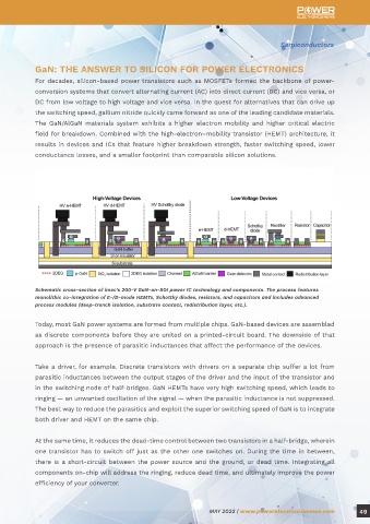
co-integration of high-performance Schottky Schematic cross-section of imec’s 200-V GaN-on-SOI power IC technology and components. The process features
monolithic co-integration of E-/D-mode HEMTs, Schottky diodes, resistors, and capacitors and includes advanced
process modules (deep-trench isolation, substrate contact, redistribution layer, etc.).
barrier diodes and D-mode HEMTs on a p-GaN
HEMT–based 200-V GaN-on-SOI smart power Today, most GaN power systems are formed from multiple chips. GaN-based devices are assembled
as discrete components before they are united on a printed-circuit board. The downside of that
IC platform. The addition of these components approach is the presence of parasitic inductances that affect the performance of the devices.
enables the design of chips with extended Take a driver, for example. Discrete transistors with drivers on a separate chip suffer a lot from
parasitic inductances between the output stages of the driver and the input of the transistor and
functionality and increased performance that in the switching node of half-bridges. GaN HEMTs have very high switching speed, which leads to
takes monolithically integrated GaN power ICs ringing — an unwanted oscillation of the signal — when the parasitic inductance is not suppressed.
The best way to reduce the parasitics and exploit the superior switching speed of GaN is to integrate
one step further. This achievement paves the both driver and HEMT on the same chip.
way toward smaller and more efficient DC/DC At the same time, it reduces the dead-time control between two transistors in a half-bridge, wherein
converters and PoL converters. one transistor has to switch off just as the other one switches on. During the time in between,
there is a short-circuit between the power source and the ground, or dead time. Integrating all
components on-chip will address the ringing, reduce dead time, and ultimately improve the power
By Stefaan Decoutere, program director of GaN power electronics at imec efficiency of your converter.
48 MAY 2022 | www.powerelectronicsnews.com MAY 2022 | www.powerelectronicsnews.com 49