
Page 11 - PEN eBook May 2022
P. 11
Cover Story – Design Cover Story – Design
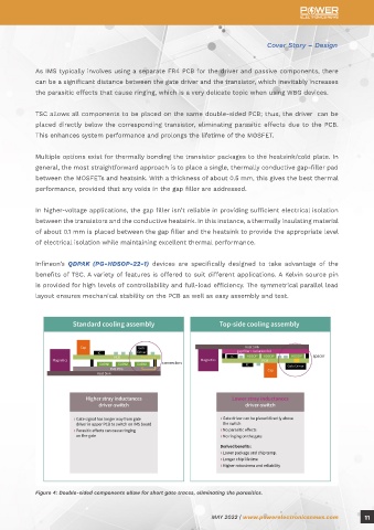
As IMS typically involves using a separate FR4 PCB for the driver and passive components, there
can be a significant distance between the gate driver and the transistor, which inevitably increases
the parasitic effects that cause ringing, which is a very delicate topic when using WBG devices.
TSC allows all components to be placed on the same double-sided PCB; thus, the driver can be
placed directly below the corresponding transistor, eliminating parasitic effects due to the PCB.
This enhances system performance and prolongs the lifetime of the MOSFET.
Multiple options exist for thermally bonding the transistor packages to the heatsink/cold plate. In
general, the most straightforward approach is to place a single, thermally conductive gap-filler pad
between the MOSFETs and heatsink. With a thickness of about 0.5 mm, this gives the best thermal
performance, provided that any voids in the gap filler are addressed.
In higher-voltage applications, the gap filler isn’t reliable in providing sufficient electrical isolation
between the transistors and the conductive heatsink. In this instance, a thermally insulating material
Figure 3: TSC permits double-sided component placement, allowing for a doubling of power density.
of about 0.1 mm is placed between the gap filler and the heatsink to provide the appropriate level
NEW THERMAL DESIGN THROUGH INNOVATIVE PACKAGE AND of electrical isolation while maintaining excellent thermal performance.
COOLING APPROACH
While acknowledging the benefits of WBG technology, designers must also be aware that improved Infineon’s QDPAK (PG-HDSOP-22-1) devices are specifically designed to take advantage of the
thermal performance plays a crucial role in achieving these important goals. benefits of TSC. A variety of features is offered to suit different applications. A Kelvin source pin
is provided for high levels of controllability and full-load efficiency. The symmetrical parallel lead
In current SMD designs, the conduction path for the heat is downward, through the legs of the layout ensures mechanical stability on the PCB as well as easy assembly and test.
component into the PCB, which is bonded to a heatsink. In challenging applications, the power
components may be mounted on an insulated metal substrate (IMS), which improves thermal
performance, as it is a better conductor of heat than standard FR4 materials. However, the natural
inclination of heat is to rise, making bottom-side cooling (BSC) seem somewhat counterintuitive.
Through innovative packaging, Infineon has developed top-side–cooled (TSC) discrete semiconductors
and ICs. This concept not only takes advantage of the natural upward flow of heat but delivers many
additional benefits that are advantageous to the OBC design and other similar applications.
In BSC, a cold plate/heatsink is typically attached to the bottom side of the PCB/IMS to dissipate
heat. This precludes the placement of components on one side, reducing power density by a factor
of 2. Also, the semiconductor devices are thermally bonded to the PCB, which means they will
operate at the same temperature. As the glass transition temperature of the FR4 PCB is lower than
the operating temperature of many WBG devices, they cannot be used to their full potential.
With the cold plate bonded to the top side of the power components, these issues are easily
addressed, allowing for components to be placed on both sides, and WBG devices can be used over
their entire operating temperature range.
Figure 4: Double-sided components allow for short gate traces, eliminating the parasitics.
10 MAY 2022 | www.powerelectronicsnews.com MAY 2022 | www.powerelectronicsnews.com 11