Page 25 - PEN eBook July 2022
P. 25
Semiconductors                                                                             Semiconductors


 to the defects and poor crystallinity. The thick buffer with low thermal conductivity adds significant
 thermal resistance to the heat dissipation path from the device to the substrate, as most of the
 heat is generated within the active layer at the top. Defect and boundary scatterings within the

 transition layer, at the interface between the substrate and transition layer, and by near-interfacial
 disorder contribute together to large thermal resistance.


 Though  there are choices of substrates  that can be used  for growing GaN epi, some are not
 foundry-friendly, whereby CMOS processes are used. Another reason is that the lithography tools
 and other tools for making CMOS devices that are state of the art are available only on larger-scale
 wafers. Hence, GaN-on-Si with wafer sizes of up to 12 inches has advantages. GaN-on-sapphire at
 6 inches is relatively inexpensive; however, many foundries do not accept sapphire, and its thermal   Figure 1: GaN manufacturing
 conductivity is poor.
            WHAT NEW TECHNOLOGIES CAN HELP SOLVE THESE PROBLEMS?

 To grow high-quality GaN, expensive substrates such as bulk GaN and SiC are required. Therefore,   Until now, there has been no easy way to remove the SiC or Si substrate from this device structure,
 the production cost for the device manufacturing is significantly higher than Si-based electronics. To   and hence, the device was very expensive.
 achieve cost-effective state-of-the-art GaN power device performance while efficiently managing
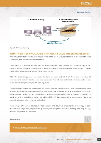
 the generated heat, the epi layer could be removed from the substrate, enabling substrate reuse,   The invention of remote epitaxy and 2D material-based layer transfer (2DLT) technology at MIT
 and  directly  bonded  to  a  heatsink  to  improve  device  thermal  performance.  However,  existing   made it possible to grow the compound materials through the 2D material. Once grown, it can be
 removal  processes  such  as  those  involving  photoelectrochemical  etching,  mechanical  spalling,   lifted off to release the substrate from it and reuse.

 and laser interface decomposition suffer from slow processing speed and/or significant surface
 roughening/cracking, limiting  the process  yield and practicality of substrate reuse.  Therefore,   With  this  technology,  one  can  create  the  GaN  epi  layer  and  lift  it  off  from  the  expensive  SiC
 the process cost of these conventional methods typically exceeds GaN substrate cost, limiting   substrate and transfer it onto a low-cost substrate. This will free up the SiC substrate to be reused
 manufacturing.  in the next GaN epi wafer growth (see Figure 1).


 When  the  device  needs  better  quality,  in  terms  of  dislocation  density,  thermal  properties,  and   The advantages of remote epitaxy and 2DLT solutions are instantaneous liftoff of the GaN thin film
 higher  frequencies  that  are  needed  for  high-voltage  devices  in  power  for  automotive,  RF,  and   without any polishing or other post-processing step. No polycrystalline or amorphous regions will
 data-center  applications,  GaN-on-SiC  tends  to  be  the  way  to  go.  However,  GaN-on-SiC  is  an   be introduced by the bonding or exfoliation process. No nucleation layer with poor crystallinity is
 expensive solution. Once the good-quality GaN epi layer is grown on the SiC substrate, you will get   required, so it is possible to obtain ultrathin (<200 nm) GaN freestanding membranes. This is not

 a better GaN device for power and RF applications. The drawback is that SiC substrates are very   possible with any other existing technology.
 expensive. The SiC substrate is no longer needed after the GaN epi layer is grown on top of it.
            The new age of GaN has started. Remote epitaxy and 2DLT are enabling the technology to scale
 To summarize:  the GaN to a larger size, improve the quality by reducing the dislocation density, and help manage
            thermal properties at low costs.
 ▶   Large GaN wafers of current technology have higher dislocation density (poor
 crystallinity).
            Reference

 ▶   GaN-on-Si wafers tend to use very thick buffers and interlayers to manage the stress,
 making it difficult to manage thermal conductivity.
                    ▶ PowerUP Expo Virtual Conference

 ▶   Most other substrates are very expensive, and scaling to larger wafers is not an option.


 28  JULY 2022 | www.powerelectronicsnews.com                       JULY 2022 | www.powerelectronicsnews.com         29

