Page 30 - PEN eBook July 2022
P. 30

Design                                                                                                                                                                                           SEMICONDUCTORS


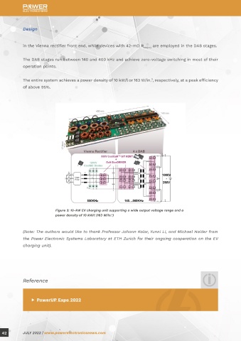
            in the Vienna rectifier front end, while devices with 42-mΩ R    are employed in the DAB stages.
                                                                        DS(on)

            The DAB stages run between 140 and 400 kHz and achieve zero-voltage switching in most of their

            operation points.


            The entire system achieves a power density of 10 kW/l or 163 W/in. , respectively, at a peak efficiency
                                                                            3
            of above 95%.


                                                                                                                                   Non-CMOS-Compatible


                                                                                                                                   SiC Power Device


                                                                                                                                   Fabrication in Volume


                                                                                                                                   Si Fabs


                                                                                                                                   Adapted from a presentation by Victor Veliadis, executive director and CTO of
                                                                                                                                   PowerAmerica and professor of electrical and computer engineering at North
                            Figure 3: 10-kW EV charging unit supporting a wide output voltage range and a                          Carolina State University
                            power density of 10 kW/l (163 W/in. )
                                                        3
                                                                                                                                   Silicon  carbide  devices  are  displacing  their  incumbent  silicon  counterparts  in  several
            (Note: The authors would like to thank Professor Johann Kolar, Yunni Li, and Michael Haider from                       high-volume  power  applications. As  SiC  market  share  continues to  grow, the  industry  is  lifting

            the Power Electronic Systems Laboratory at ETH Zurich for their ongoing cooperation on the EV                          the last barriers to mass commercialization that include higher-than-Si-device cost, relative lack
            charging unit).                                                                                                        of wafer planarity, the presence of basal plane dislocations, reliability and ruggedness concerns,
                                                                                                                                   and the need for a workforce skilled in SiC power technology to keep up with the rising demand.
                                                                                                                                   To enable cost-effective SiC manufacturing, high-yielding fabrication processes are required. In
                                                                                                                                   my PowerUP presentation, I will summarize key aspects of SiC fabrication technology and outline
                                                                                                                                   non-CMOS-compatible  processes  that  have  been  streamlined  to  allow  for  mass  SiC  device
            Reference                                                                                                              fabrication in conventional mature Si fabs.


                                                                                                                                   SiC WAFERS

                    ▶ PowerUP Expo 2022                                                                                            Today, the  SiC wafer  represents  55% to 70%  of the  overall  SiC  device  cost,  a  consequence  of  its
                                                                                                                                   uniquely complex fabrication specifics. Conventional SiC substrates are primarily grown by the seeded
                                                                                                                                   sublimation technique at temperatures of ~2,500˚C, which creates process control challenges. Crystal


  42        JULY 2022 | www.powerelectronicsnews.com                                                                                                                                       JULY 2022 | www.powerelectronicsnews.com         43
   25   26   27   28   29   30   31   32   33   34   35