Page 34 - PEN Ebook May 2021
P. 34
Design                                                                                                                                                                                                               Design


                                                                                                                                 Figure 2: CL filter Waveform.


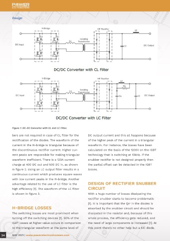
          Figure 1: DC-DC Converter with CL and LC Filter.

          bers are not required in case of CL filter for the   DC output current and this all happens because
          rectification of the diodes. The waveform of the     of the higher peak of the current in a triangular
          current in the H-bridge is triangular because of     waveform. For instance, the losses have been
          the discontinuous rectifier current. Higher cur-     calculated on the basis of the 1200V on the IGBT

          rent peaks are responsible for making triangular     technology that is switching at 10kHz. If the
          waveform inefficient. There is a 120A current        snubber rectifier is not designed properly then
          charge at 400 DC out and 500 DC in, as shown         the partial offset can be detected in the IGBT
          in figure 2. Using an LC output filter results in a   losses.
          continuous current which produces square waves
          with low current peaks in the H-bridge. Another
          advantage related to the use of LC filter is the     DESIGN OF RECTIFIER SNUBBER

          high efficiency [1]. The waveform of the LC filter   CIRCUIT                                                           Figure 3: LC filter Waveform.
          is shown in figure 3.                                With a huge number of losses dissipating the                      ADVANTAGES OF SIC SCHOTTKY                            ▶   Small amount of charge at the capacitance of
                                                               rectifier snubber starts to become problematic                    DIODE                                                    the junction, but it is not greater than the Qrr
                                                               [1]. It is important that the Qrr in the diodes is                Some of the significant advantages that are as-          at the normal Si PN junction.
          H-BRIDGE LOSSES                                      absorbed by the snubber circuit and should be                     sociated with the SiC devices are:

          The switching losses are most prominent when         dissipated in the resistor and, because of this                                                                         ▶   Easy and ready availability at the standard
          turning off the switching devices [1]. 50% of the    whole process, the efficiency gets reduced, and                    ▶   A tendency of lowering the loss of switching.       package of the industry.
          IGBT losses at higher value occurs in comparison     the need of large components is increased [1]. At
          to the triangular waveform at the same level of      this point there’s no other help but a SiC diode.                  ▶   Reverse recovery charge is not present.


  34      MAY 2021 | www.powerelectronicsnews.com                                                                                                                                              MAY 2021 | www.powerelectronicsnews.com      35

