
Page 55 - PEN Ebook March 2021
P. 55
SEMICONDUCTORS Semiconductors
SIC FETS ARE AN ALTERNATIVE slow edge rates for these types of fast switches,
CHOICE allowing perhaps the use of lower voltage devices
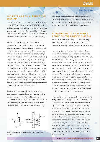
The UnitedSiC FET is a cascode combination of with better conduction losses and smaller filters,
a SiC JFET and a low voltage Si MOSFET which offsetting the slightly higher switching losses.
yields a device with all the speed and harnesses
the lowest conduction loss benefits of SiC but
with an easy gate drive and a fast, low loss body SLOWING SWITCHING EDGES
diode for third quadrant conduction (Figure 1). REDUCES OVERSHOOT AND EMI
There are two common ways to slow switching
SiC FETS are blazingly fast with edge rates of edges: by adding gate resistance and by using a
50V/ns and higher which is great to minimize snubber across the devices’ Drain-Source terminal.
switching losses, but the resulting di/dt can be
many amps per nanosecond. This, through pack- Increasing gate resistance does reduce dV/dt,
age and circuit inductances can produce high reducing overshoot, but is shown to have little
levels of voltage overshoot and subsequent ring- effect on subsequent ringing of the Drain voltage.
ing. At these rates of change of current, simple The slowing effect of the gate resistor depends
analysis tells us that even a few tens of nano- on total gate charge for the device which in turn
henries can produce hundreds of volts of over- depends on parameters such as Gate-Source ca-
shoot (from E = - L.di/dt). Minimizing this stray pacitance and the ‘Miller’ effect, which appears
inductance is essential for fast switching WBG as a varying Gate-Drain capacitance as the device
devices, however, this is difficult to implement switches. Turn-on and -off delays can be sepa-
in practical layouts that have to achieve safety rately controlled by using two Gate resistors with
clearances between high voltage components, diode-steering, but the overall effect is difficult
and that use larger semiconductor packages for to optimize conditions over all operating condi-
their better thermal performance. tions. Additionally, adding gate resistance intro-
duces a delay to the gate drive waveform which
Overshoots risk exceeding voltage rating of can be problematic at high frequency.
Minimizing EMI and devices, and increase long-term stress on the In contrast, simple Rs-Cs snubbers can slow dV/
components, but the fast edges also provoke
switching loss in SiC insulation breakdown and tend to produce more dt by effectively adding capacitance to the drain
EMI, requiring bigger, costlier and lossy filters.
of the switch. An additional effect is that over-
FETs Practical circuits therefore often deliberately lap between voltage rising and current falling
on turn-off is reduced, as some of the current
is diverted into charging Cs, decreasing device
By Peter Losee, Director of Technology Development, UnitedSiC switching loss. The capacitor discharge current
must be limited when the switch turns on, so
a resistor is added in series which also serves
In the new era of wide band-gap semiconductor quite yet, with both device types having limita- to damp ringing as the device turns off. The
switches, the choice of device types includes SiC tions in some areas, particularly in their particu- downside is that the resistor inevitably dissi-
MOSFETs and GaN HEMT cells, both with their lar gate drive requirements and ‘third quadrant’ pates some power in the process and the gain
own characteristics and claims to best perfor- operation. in switching efficiency in the semiconductor is
Figure 1: The SiC FET – a cascode of a SiC JFET and Si
mance. However, neither are the ideal switch MOSFET. offset to an extent.
54 MARCH 2021 | www.powerelectronicsnews.com MARCH 2021 | www.powerelectronicsnews.com 55