
Page 56 - PEN Ebook March 2021
P. 56
Semiconductors Semiconductors
(a) VDS peak during turn-off, the snubber version
clearly shows shorter delay times and better
damping of the ringing.
Overall loss is a combination of conduction loss,
device switching loss on rising and falling edges
and any power dissipated in the snubber resistor.
Making the comparison with SiC MOSFET devic-
es, tests at UnitedSiC show that at high drain
current, turn-off energy lost, EOFF, with a snub-
ber solution can be 50% of the loss when peak
(b)
voltage is equivalently tuned with a gate resistor
alone. Meanwhile turn on energy, EON, is mar-
ginally higher, (only around 10%), so that for an
example 40 milliohm device switching at 40kHz
and 48A/800V, the net effect is a total bene-
fit with the snubber of around 275µJ per cycle
or 11W. This comparison is shown in Figure 3 as
the blue and yellow plots. The black plot is the Figure 3: Comparing total switching losses of SiC switches with and without snubbers.
performance of a 40 milliohm UnitedSiC SiC FET
device with snubber and optimized gate -on and have a Kelvin connection to the source, effec- ber networks. However, wide band-gap devices,
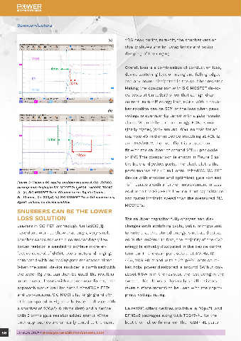
Figure 2: Using a RC device snubber reduces dV/dt, ID/VDS -off resistors with a further improvement in loss- tively eliminating the effect of source induct- particularly SiC FETs, can use the technique as
overlap and ringing in SiC MOSFETs I =50A, V=800V, TO247-
D
4L (a) SiC MOSFET Turn-Off waveform, Rg,off=0ohms, es due to the SiC FET’s lower output capacitance ance, improving switching losses and resulting in a superior alternative to gate resistor tuning to
Rs=10ohms, Cs=200pF, (b) SiC MOSFET Turn-Off waveforms, and faster intrinsic speed than the measured SiC cleaner gate waveforms at high drain di/dt. provide overall lower losses and can be imple-
Rg,off=5ohms, no device snubber
MOSFETs. mented with compact, inexpensive components.
SNUBBERS CAN BE THE LOWER
LOSS SOLUTION The snubber capacitor fully charges and dis- CONCLUSION
Leaders in SiC FET technology, UnitedSiC[1], charges each switching cycle, but it is important Device snubbering might seem to be a ‘brute-
have done work to show that only a very small to note that this stored energy is not all dissipat- force’ solution to managing switch overshoot,
snubber capacitor with a correspondingly low ed in the resistor. In fact, the majority of the CV2 ringing and losses, and this is certainly the case
power resistor is needed to achieve more ef- energy is actually dissipated in the device during with older technologies such as IGBTs, with their
fective control of dV/dt, overshoots and ringing, turn-on. In the example quoted, at 40kHz, ID long ‘tail currents’, requiring large and lossy snub-
compared with increasing gate resistance alone. 40A, VDS 800V and with a 220pF/10 ohm snub-
When the small device snubber is combined with ber, total power dissipated is around 5W but only
the lower Rg that can then be used, the result is about 0.8W is in the resistor, the rest being in the For More Information
lower overall losses with cleaner waveforms. This switch. This allows a physically small resistors
approach works well for both UnitedSiC’s FETs (even surface mount) to be used with the appro- ▶ Silicon Carbide (SiC)
and conventional SiC MOSFETs. Ringing and dV/ priate voltage rating.
dt is compared in Figure 2 between a device with ▶ (PC9) Achieving optimal performance: Minimizing EMI and switching loss for SiC
a snubber of 200pF/10 ohms (left) and a device UnitedSiC offers devices available in D2pk7L and
with 5 ohms gate resistor added (right). While DFN8x8 packages along with TO247-4L for the FETs – Talk at Power Forum
both approaches are similarly tuned to the same best thermal performance. The TO247-4L parts
56 MARCH 2021 | www.powerelectronicsnews.com MARCH 2021 | www.powerelectronicsnews.com 57