
Page 15 - PEN Ebook March 2021
P. 15
Semiconductors Semiconductors
in catastrophic failure.
Besides overstress on the enabled gate, disa-
bled gates can be affected too. If the V >V , ID
GS
th
starts flowing in the disabled device. The shoot-
through current will lead to further excitation of
the resonant tank and a self-sustained oscilla-
tion with shoot-through currents can occur. This
is show in Figure 2.
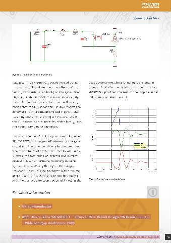
Figure 3: schematic for simulation.
Often, designers try to mitigate these oscilla-
Figure 1: Reverse Recovery current SiC MOSFET.
tion effects by adding an external C capacitor real gate. The external C builds an additional best possible switching. Enabling transients in
GS
GS
Why do you need to pay attention to the SiC (impact seen in Figure 2). This capacitor conven- resonance tank and worsens the effects of the excess of 120 V/ns and 6 A/ns (with best in class
MOSFET gate? Despite having a conventional SiO iently dampens away oscillations and seems to fast I transients (snap back) on the gate. Using MOSFETs), provided the rest of the loop parasitic
RR
2
gate oxide, this oxide has worse properties than fix the problem, or so it seems. What is overseen physical, scalable SPICE models one can study inductance is taken care of.
the classical Si-SiO interface found in conven- is the fact that the dampening and the resulting these difficult to probe effects and will quickly
2
tional Si based semiconductors. This is due to clean oscilloscope pictures are resembling the notice that the C capacitor. Figure 3 shows the
GS
intrinsic defects at the interface of SiO grown events outside the real gate, what the designer schematic for the simulations and Figure 4 the
2
on the Si terminated face of SiC. This makes the is doing in reality is worsening the effects on the resulting outcome, showing a 7 V overstress on
oxide more susceptible to over voltage, and other the V caused by the interplay of the fast I and
GS
RR
electric stress limiting the V GSMax considerably the added dampening capacitor.
relative to Si based devices.
The key to successful high speed switching using
Figure 1 shows the snappy body diode of a SiC SiC MOSFETs is a proper adjustment of the gate
MOSFE, the small Q and the short trr can be circuit and the drive conditions to the used de-
RR
tricky to measure and are often convoluted with vice, a careful read of the data sheets will quick-
the test systems parasitic capacitances. How- ly reveal the fast range of internal RGs current
ever di/dt of >40 A/ns in the I return leg can devices have. Furthermore, removing external
RR
occur. This ultra-fast I event can pull the V on C capacitors, setting the right external gate
GS
GS
RR
the device itself up in excess of Volts and cause resistor R , and utilizing packages with a source
G
severe overstress during each turn on cycle. sense (TO-247-4L, D2PAK-7L or similar), paired
The resulting overshoot is proportional to the I Figure 2: Switching transient of SiC MOSFET at: with the correct gate loop design will yield in the Figure 4: analysis of simulation.
RR
speed; eventually this continues stress will result V =720V, I =20A, T =175°C, R =10Ω, C =10nF.
DD D C G GS
For More Information
▶ ON Semiconductor
▶ (S15) How to kill a SiC MOSFET – Errors in Gate Circuit Design, ON Semiconductor
– Wide bandgap Conference 2020
14 MARCH 2021 | www.powerelectronicsnews.com MARCH 2021 | www.powerelectronicsnews.com 15