
Page 18 - PEN Ebook March 2021
P. 18
Power Supply SEMICONDUCTORS
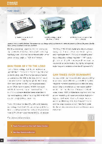
Figure 2: 400 V ¼-brick designs: The single-PCB GaN design using Navitas NV6117 GaNFast power ICs has 2x the power density
(W/cc) of any Si-based converter. [Navitas].
400 kHz operating frequency, with efficiency as 100 W/cc (1700 W/in3). Getting to the processor
high as 94.5% at full load. With a soft-switching voltages (as low as 0.6V at over 100A) requires
topology, over 1 MHz can be achieved with further new topologies from 48V-1.xV, or adopting new
power density target of 1 kW in a ¼-brick. fully-integrated voltage regulator ‘FIVR’ topolo- Correct use of parallel
gies pioneered by the Intel Haswell processor and
advanced in similar fashion by highly-integrated, GaN transistors
GAN FROM 48 V TO THE LOAD high-frequency solutions like the Empower IVR.
For the lower-voltage distribution network, an By Yalcin Haksoz, Principal Engineer, Infineon Technologies
upgrade from 12 V to 48 V means a 16x reduction
in distribution loss. This change was pioneered GAN TAKES OVER (SUMMARY)
by companies like IBM in the Blue Gene/P super- As data center traffic accelerates, silicon’s ability It is wide bandgap (WBG) technology that is pro- tween the devices due to different gate thresh-
computer in 2007 and by Google for their Hong to process power effectively and efficiently hits viding the answers as power converter designers olds, PCB trace impedances, etc. during dynamic
Kong data center in 2014. As the power need- ‘physical material’ roadblocks and the old, slow, search for approaches to attain a further single switching must also be considered. Failure to do
ed for GPUs has increased, NVIDIA have also silicon chip is overtaken by high-speed gallium percentage point of efficiency and increase the so can lead to undesirable high-frequency oscil-
switched their GPU-module input rail from 12 V nitride. The consolidation of data center hard- power density of their designs. Gallium nitride lations, challenges fulfilling EMC requirements,
to 48 V – a change that has been extended to ware, a new HVDC architecture approach and the (GaN) transistors are increasingly becoming the and even destruction of the switches.
high-end laptops, with a matching 300 W AC-48V proven reliability of mass-production, highly-in- solution but, like their silicon counterparts, single
adapter using GaNFast power ICs. tegrated GaN power ICs enable major improve- devices still have upper limits to their current While parallel operation of silicon MOSFETs is
ments in efficiency. This ‘fast-forward’ means handling capability. Use of such devices in par- well understood, the driving of a single GaN
From ~48 V down to the CPU, GPU and memory, another step towards carbon ‘Net-Zero’ goals allel is a common approach, but engineers can’t HEMT will be a new experience for many engi-
low-voltage GaN (<=80 V) can be deployed. For a for the whole power electronics and data center simply swap out silicon MOSFETs for GaN devic- neers. Due to their exceptional switching speeds,
48 V - 6 V down conversion, GaN achieves 300 W industries. es. this challenge must be well understood before
from a 27 x 18 mm open-frame DCX (LLC) at over tackling parallel operation.
For More Information SWITCHING DEVICES IN Infineon CoolGaN™ 600 V HEMT makes use of
PARALLEL AND THE OPTIMAL p-doped GaN beneath the gate, resulting in a
DRIVE pn-diode with a forward voltage of around 3.5 V
▶ Fast-Forward to the GaN Data Center
Ideally, when using parallel switches, the R DS(on) of in parallel with the gate’s capacitance C . This
G
the devices used need to be closely matched to requires a drive circuit unlike those used with
▶ Navitas Semiconductor ensure the static current flowing is spread equal- silicon MOSFETs. The diode clamps the gate to a
ly across the transistors. Lack of symmetry be- value close to V , meaning a negative voltage is
F
18 MARCH 2021 | www.powerelectronicsnews.com MARCH 2021 | www.powerelectronicsnews.com 19