Page 12 - PEN Ebook March 2021
P. 12

Cover Story - Design                                                                                                                                                                                  SEMICONDUCTORS


                                                                                                                                 How to kill a SiC MOSFET


                                                                                                                                 – Errors in Gate Circuit


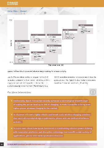
          Figure 5: Infineon/Spark Connected reference design roadmap for wireless charging.
                                                                                                                                 Design and their impact

          ure 5). The solution portfolio ranges from a 2 W     100 W inductive solution for robots and industrial
          inductive solution for low-power IoT devices (The    applications (The Ogre). It also features resonant
          Pegasus) over a 10 W inductive solution for sub-     solutions for more positioning flexibility.                       on robustness
          surface smartphone charging (The Kraken) to a

                                                                                                                                 By Mehrdad Baghaie Yazdi, Martin Warnke, ON Semiconductor
          For More Information

                                                                                                                                 The emergence of SiC MOSFETs in various topol-       dampening oscillations on the gate, in order to
                                                                                                                                 ogies has resulted in great performance and          improve switching transients actually results in
                 ▶ Additionally, Spark Connected recently achieved a technological breakthrough                                  efficiency improvements. However, if not used        heavy stress on the gate. This stress is not easily
                of scaling the power level up to 300 W charging. It made it possible to bring even                               correctly, engineers can quickly find themselves     visible through measurements, as they occur on
                                                                                                                                 frustrated with device failures. These failures      the internal gate node and not on the external
                higher-power wireless charging to the market.
                                                                                                                                 are often, quite in contrast to the perception of    measurable one which, thanks to the C , seems
                                                                                                                                                                                                                            GS
                                                                                                                                 the customers, not intrinsic weaknesses of the       nicely dampened. Furthermore, we discuss the
                 ▶ To discover Infineon's highly reliable and broad-scale wireless charging solutions
                                                                                                                                 SiC MOSFET technology but in the design choic-       attention that has to be given to the SiC MOS-
                that meet all essential design requirements, please visit our dedicated Infineon                                 es around the gate loop. Particularly the lack of    FET body diode. There are many misconceptions

                website.                                                                                                         attention to the turn-on interactions between the    around the body diode of SiC MOSFETs, to the
                                                                                                                                 high side and low side device can result in cata-    point that even veteran technologists sometimes
                 ▶ To learn more about how Spark Connected is transforming wireless power delivery                               strophic failures excited by wrong circuit choices.   believe that this body diode is reverse recovery
                                                                                                                                 In this paper, we show that classical dampening      free. Indeed, we show that the body diode of SiC
                with innovative platforms and disruptive technology that benefit a wide variety of
                                                                                                                                 efforts using gate source capacitors in the gate     MOSFETs, in particular planar gate devices, can
                applications, please visit www.sparkconnected.com.
                                                                                                                                 circuit loop are a great hazard and an often-hid-    be a culprit in causing damage to the gate.
                                                                                                                                 den killer of SiC MOSFET gates. This practice of


  12      MARCH 2021 | www.powerelectronicsnews.com                                                                                                                                         MARCH 2021 | www.powerelectronicsnews.com       13
   7   8   9   10   11   12   13   14   15   16   17